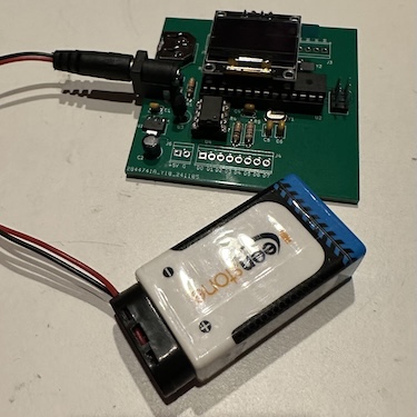
Below are steps for building verson 1 of the Temp-time project.
For anyone who has made a Cyduino, this build should be familiar. Of course, there are extra components that provide the time and temperature functionality and the display.
The order of assembly given below is a suggestion, but there is nothing wrong with soldering the parts in a different order.
A new thing regarding soldering is the use of one surface-mount component, the 5-V regulator chip. All earlier projects used 74xx-style regulators in large TO-220 through-hole packages. For this project, we use STMicroelectronics LD1117 regulator in an SOT-223 package, which is one of the easier surface mount packages to solder by hand. This should be a gentle introduction to surface-mount technology.
The usual tools are required: solder and soldering iron, needle-nosed pliers for manipulating parts and pulling leads, and wire cutters for trimming leads after soldering. Helpful but not essential would be a vise for holding the boards, a magnifying glass and light for viewing small print, and tweezers for holding the surface-mount part in place during soldering.
- Assemble the parts. (See the BoM for the complete list.)
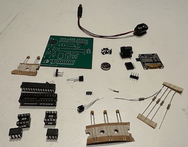
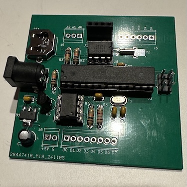
- Solder in the three sockets — 28 pin for Atmega chip and 8 pin for the real-time clock and op-amp chips. (Note: The 8-pin sockets from the kit may look slightly different than those in the photos.)
Remember that sockets are optional. If you want to live dangerously, you can solder the chips directly to the board. But if something goes wrong with the chips, they will be difficult to remove. If you decide to solder directly to the board, it is probably better to wait and install them as the last step in the assembly.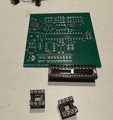
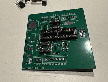
- Add the two 100-nF (104) by-pass capacitors. These are labeled C3 and C4 on the board.
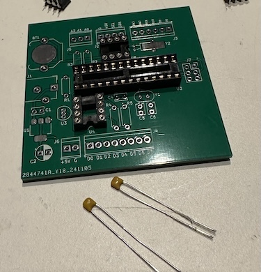
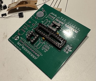
- Next solder in the oscillator crystal for the Atmega (labeled Y1 on the board) and the accompanying 22-pf (22J) capacitors (labeled C5 and C6).
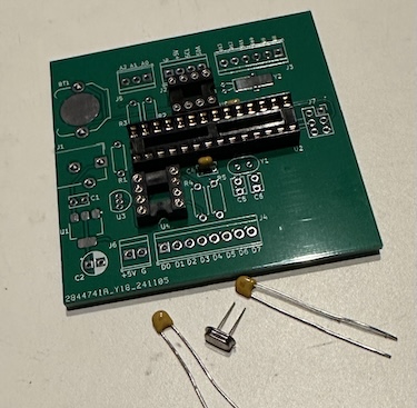
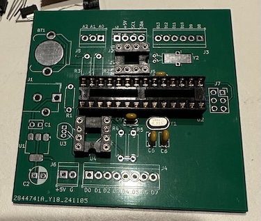
- Now add three 10-kΩ pull-up resistors. One is the pull up for the Atmega reset pin (labeled R1) and the other two are pull ups for the serial communications channel used by the real-time clock and the display (labeled R2 and R3).
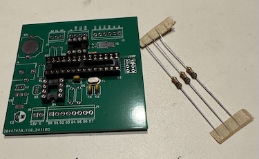
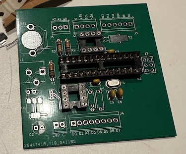
- Next, solder in the two resistors that form the feedback network for the op amp. Don't mix these up! R4 is a 10-kΩ resistor (brown-black-orange) and R5 is 1.8 kΩ (brown-gray-red).
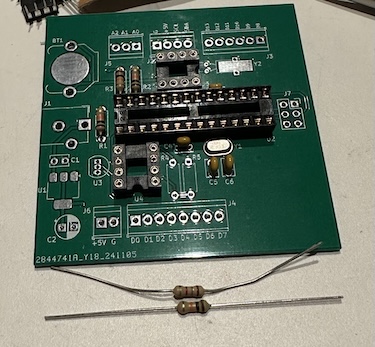
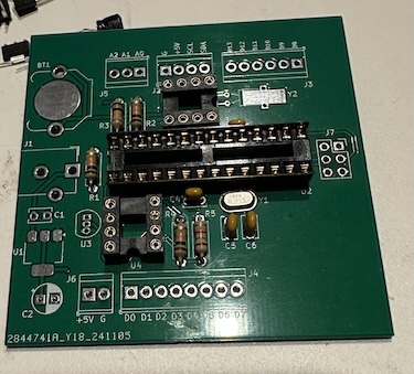
- Put in the 32.768-kHz crystal for the RTC. Polarity does not matter. Note that the part is quite small, and the footprint on the board is clearly the wrong size — not an elegant look. (Something to be fixed in version 2.) But the crystal should work just fine.
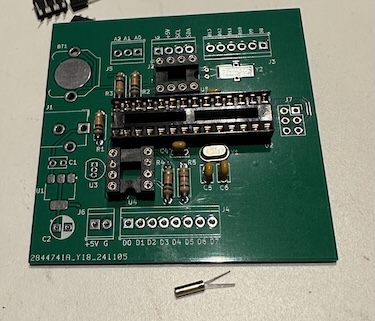
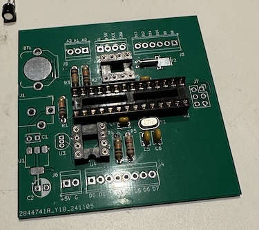
- Now come the three components for the voltage regulator — the LD1117 chip (U1 on the board) and two capacitors. The 100-nF (104) cap is labeled C1 and the 10-μF electrolytic cap is labeled C2. Note that polarity does not matter for C1, but it does for C2. Make sure that the negative terminal for C2 (negative sign inside the gray area) aligns with white area on the PCB footprint.
Suggested approach for soldering the surface-mount chip: First melt some solder onto one of the pads in the footprint. (It doesn't matter which pad.) Then carefully align the chip leads with the pads and hold the chip in place. (Using pliers or tweezers to hold the chip is helpful.) Then use the soldering iron to remelt the solder on the one pad so that it reflows around the lead. Remove the iron and let the solder cool. Check the alignment of the leads to the pads. If the chip has slipped and the pads are not aligned, remelt the solder and move the chip to attain better alignment. Repeat as necessary. Once everything is aligned, solder the remaining leads to the pads.
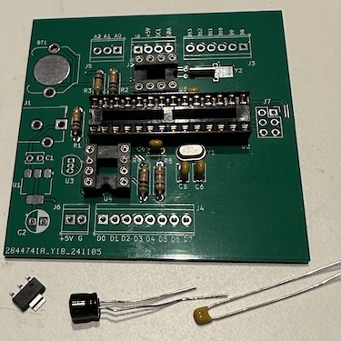
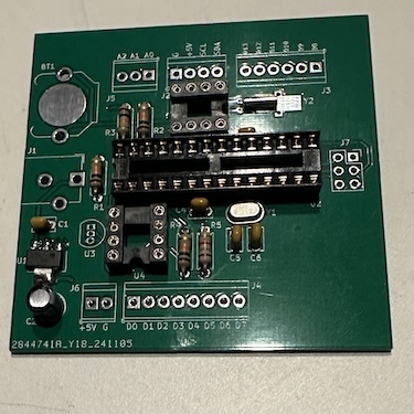
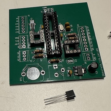
- Next, add the LM32 temperature sensor (labeled U3 on the board). Again, polarity is important. Note that the package has a flat edge and the outline on the board shows where the flat edge should go. It may be necessary to fiddle with the leads a bit to align them with the holes on the board. You can insert the sensor until is flush with the board or it can be left "standing proud" a bit above the board, as was done here. The might give slightly better temperature performance, but any difference is probably negligible.
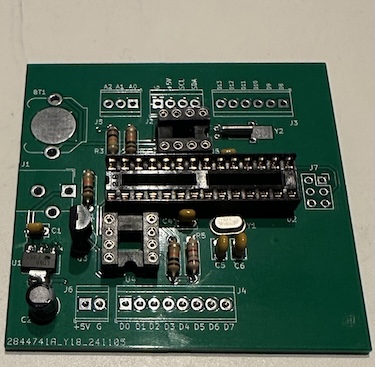
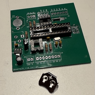
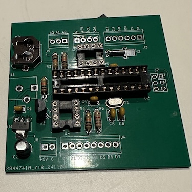
- Now we can place the battery holder for the RTC backup battery. There's nothing tricky here.
- And the barrel connector for power from the battery or plug-in supply.
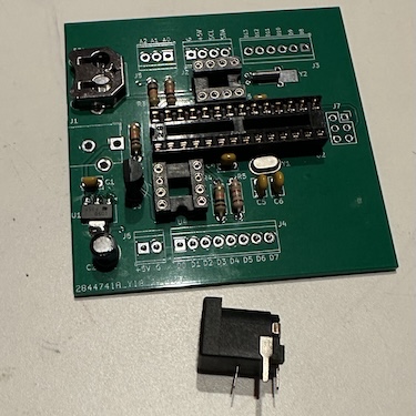
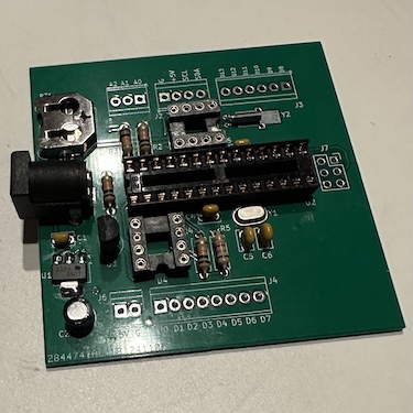
- Solder in the standoff for the display (label J2 on the board) and the ICSP header (labeled J7).
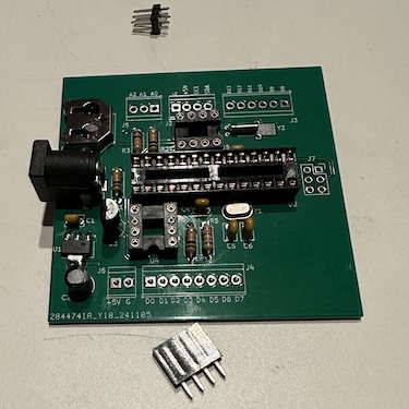
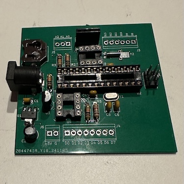
- Heading for the finish, we can insert the three DIP chips. The MPC601 op amp is labeled U4 and the 1307+ RTC is U5. Accidentally swapping these two would be bad. As always, it may be necessary to bend the pins a bit to get everything aligned. Don't force it! If you are not planning to use the ICSP to program the Atmega, then don't forget to load the program before plugging it into the socket
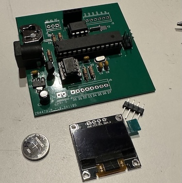
- Finally! Solder the header pins to the OLED display. (Make sure the long end of the pins are pointing down, away from the front of the display.) Insert the display into the header. Insert the 2012 backup battery.
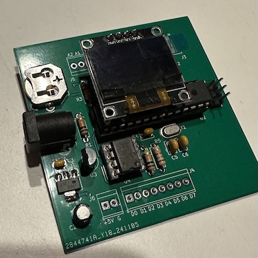
- Power it up with a 9-V battery or a 9-V plug-in supply. It is always a good idea to use a meter to check power supply voltages at a few key spots in the circuit — voltage-regulator output, power-supply pins on the chips, etc.
