ISU Audio and Arduino Club
Cyduino build instructions
- Below are step-by-step instructions for building the Cyduino project. If you have soldered together any of the other Arduino Club projects, the Cyduino will be familiar.
- The order of assembly given below is merely a suggestion — there is nothing wrong with soldering the parts in a different sequence.
- Some components in the photos may appear different from those in the kits. The parts used here are from my personal parts bin at home, not from one of the kits.
- The usual tools are required: solder and soldering iron, needle-nosed pliers for manipulating parts and pulling leads through holes, and wire cutters for trimming leads after soldering. Helpful but not essential would be a vise for holding the boards and a magnifying glass and light for viewing small print.
- The images are links; click on them to open a higher resolution photo in a new window.
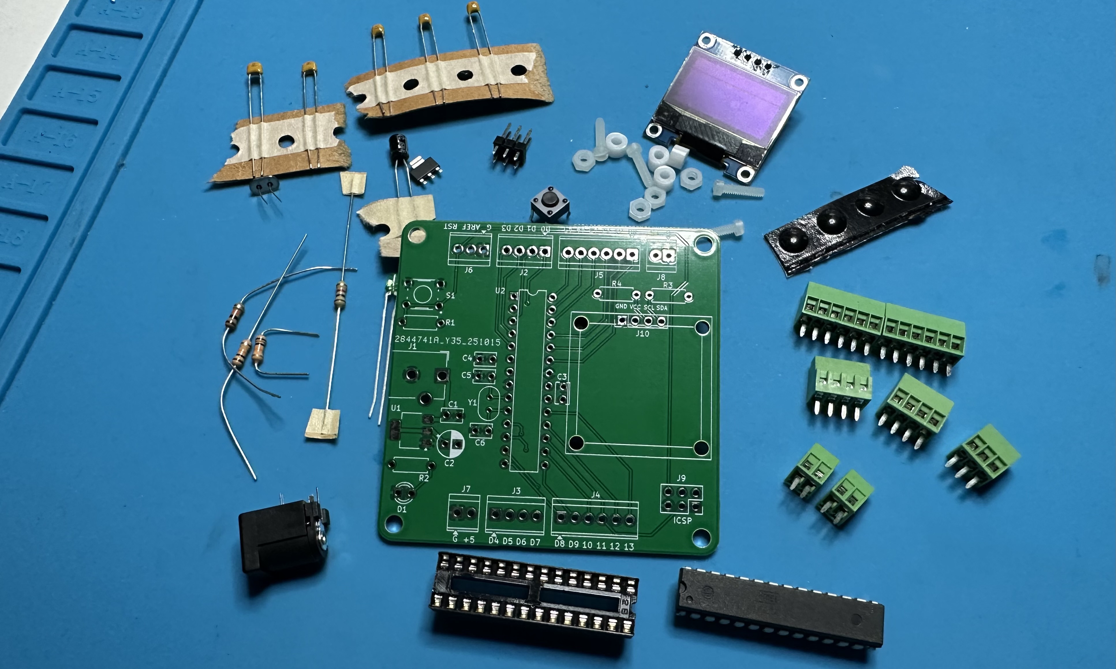
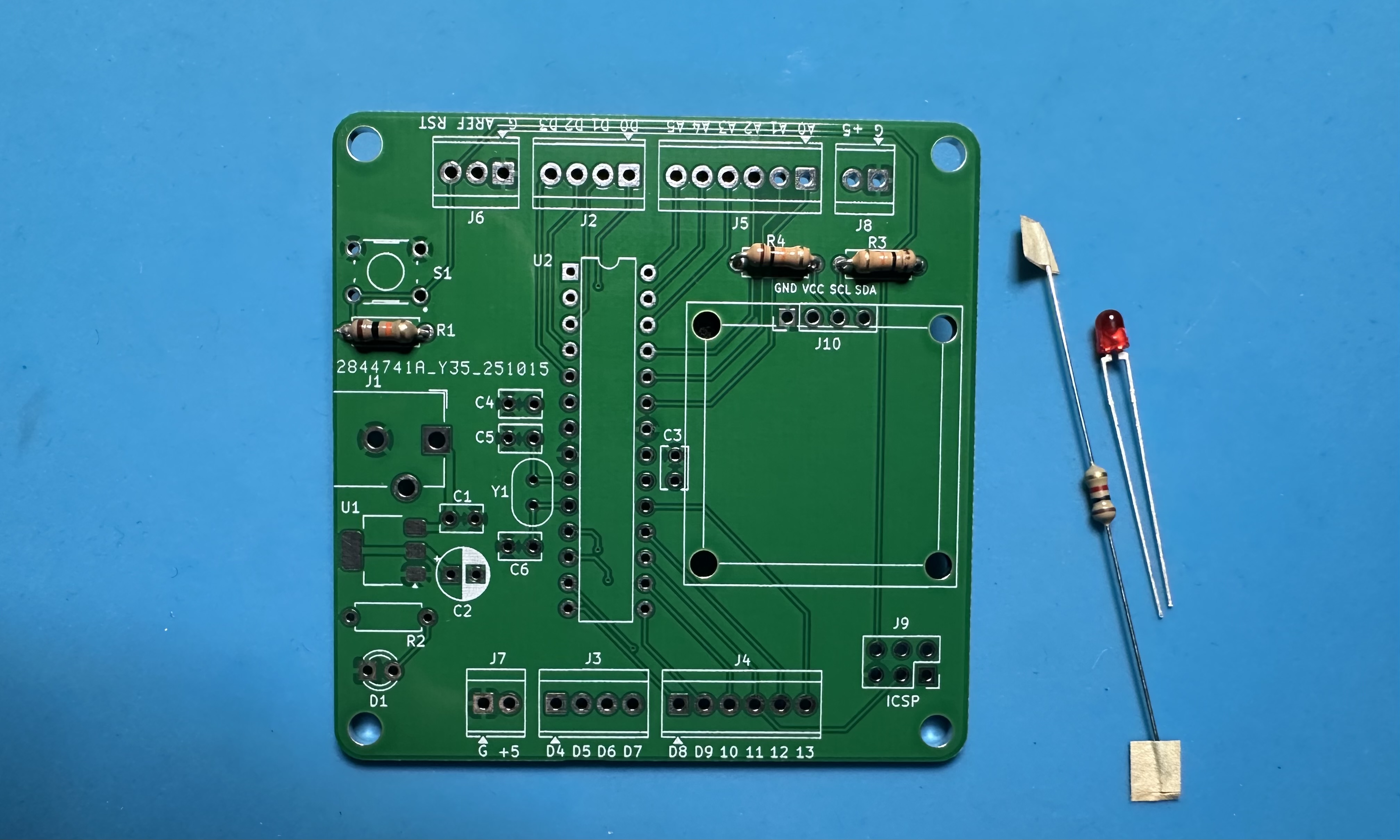
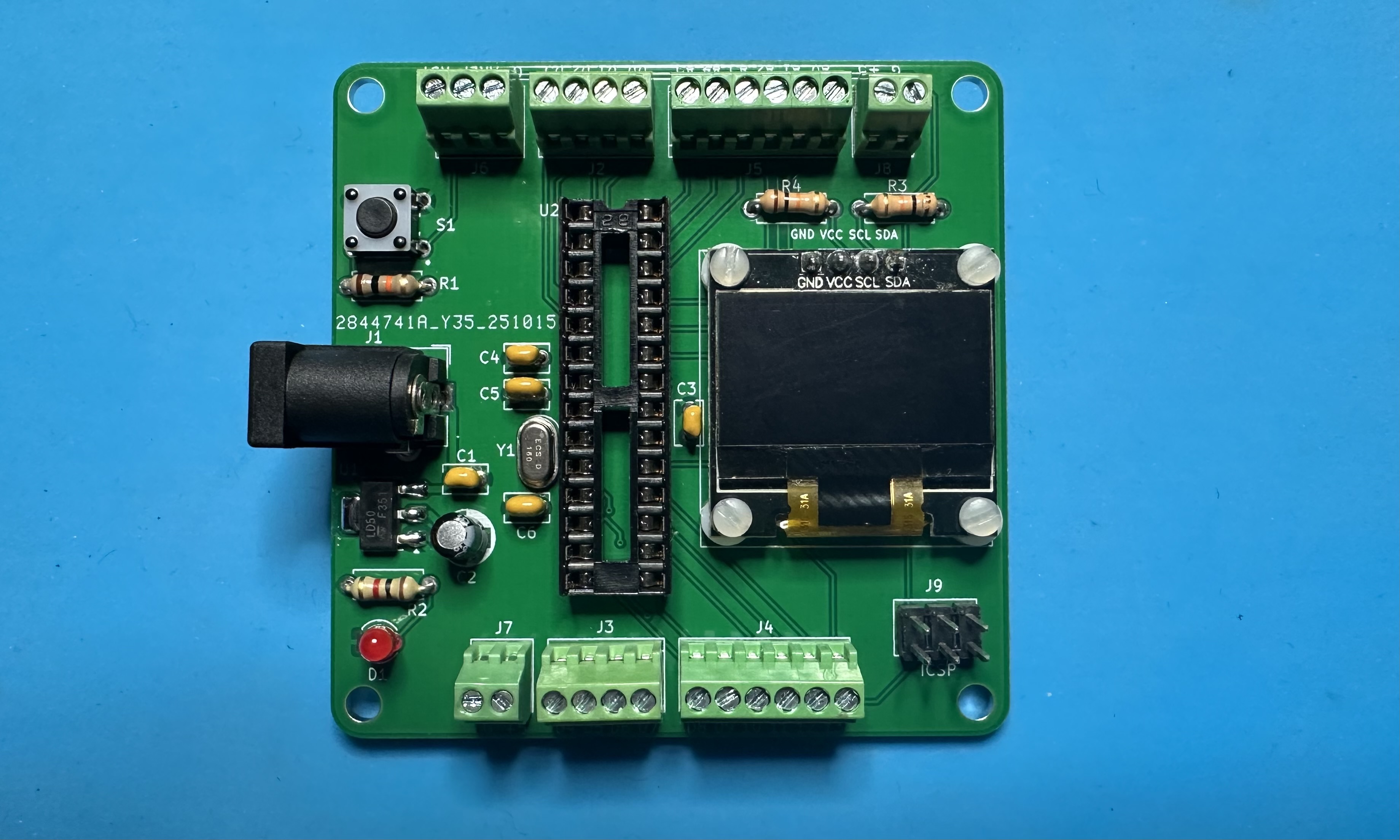
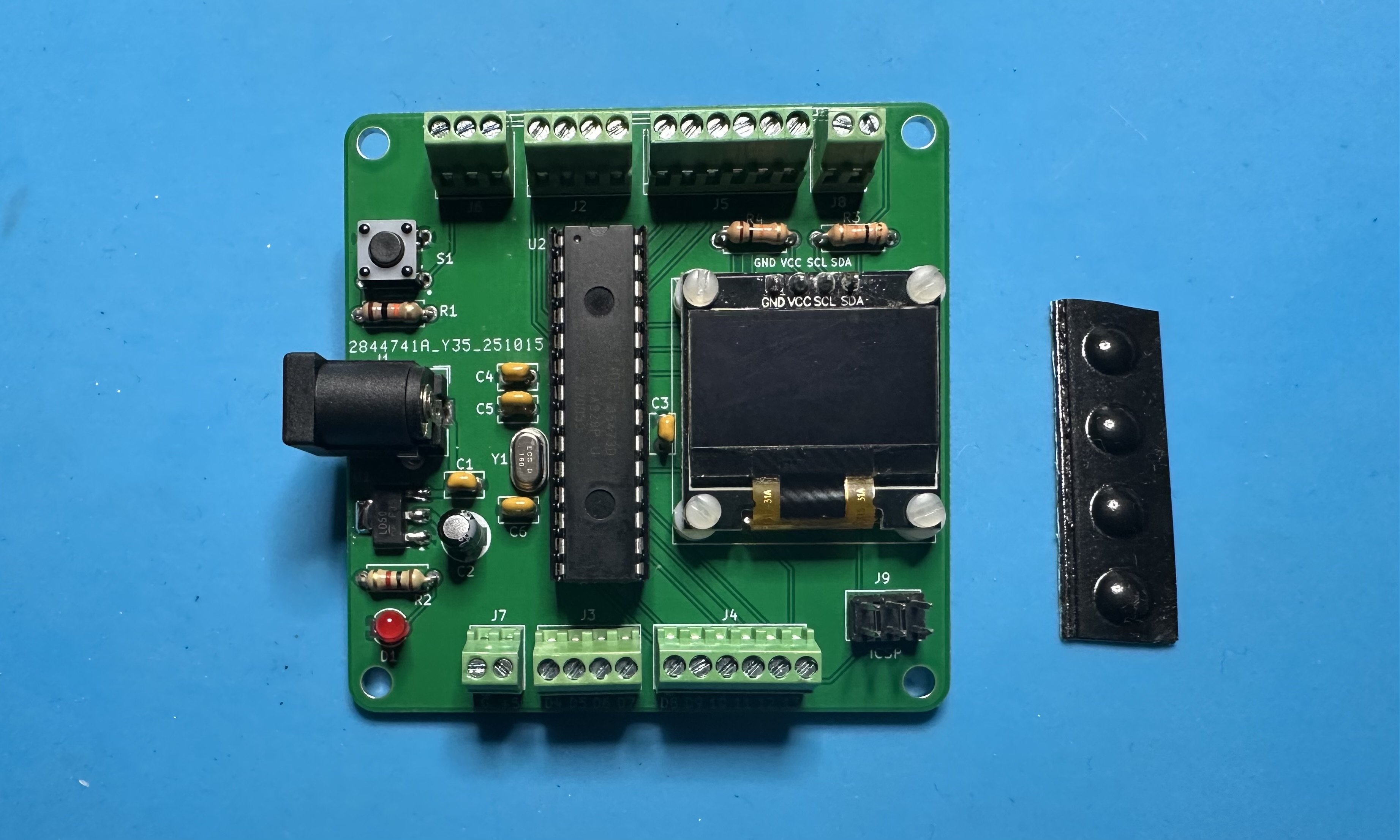
- Assemble the parts. (See the BoM for the complete list.)
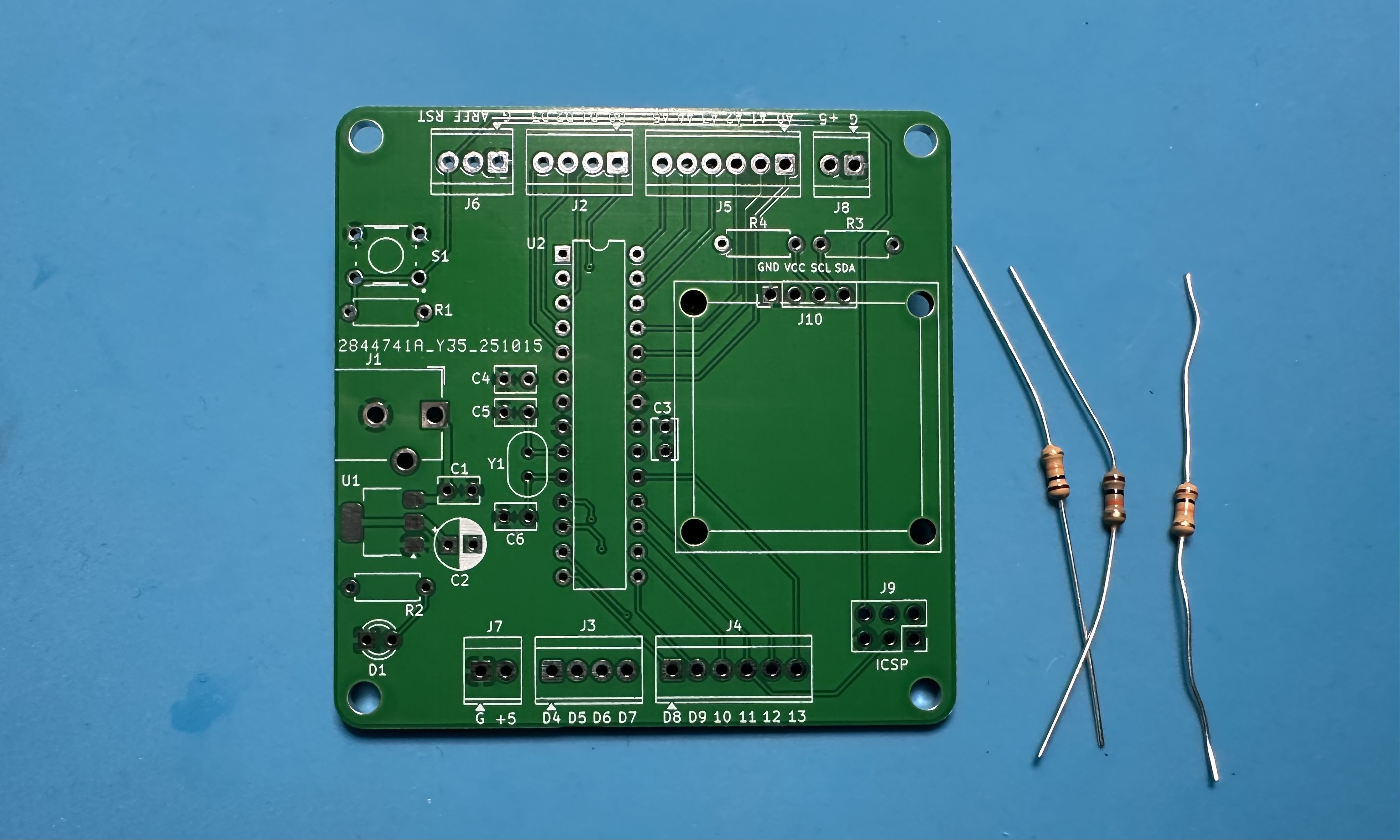
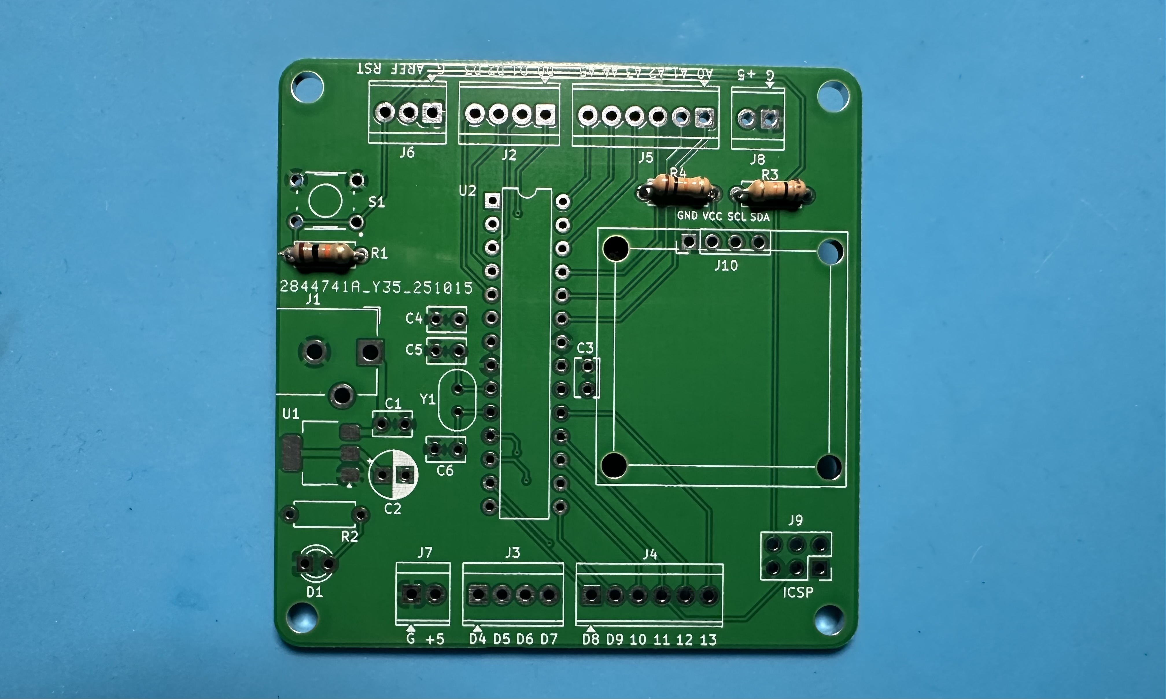
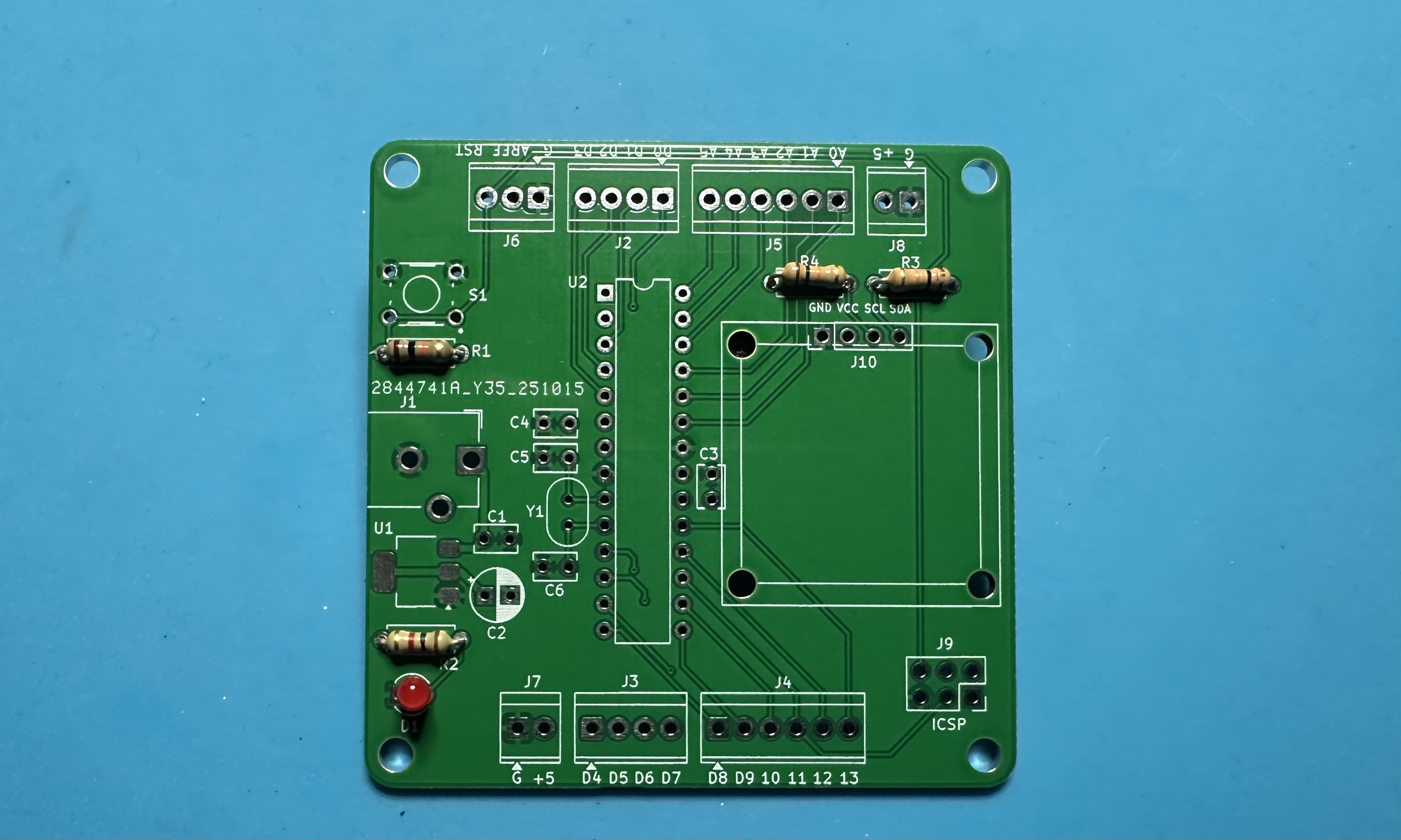
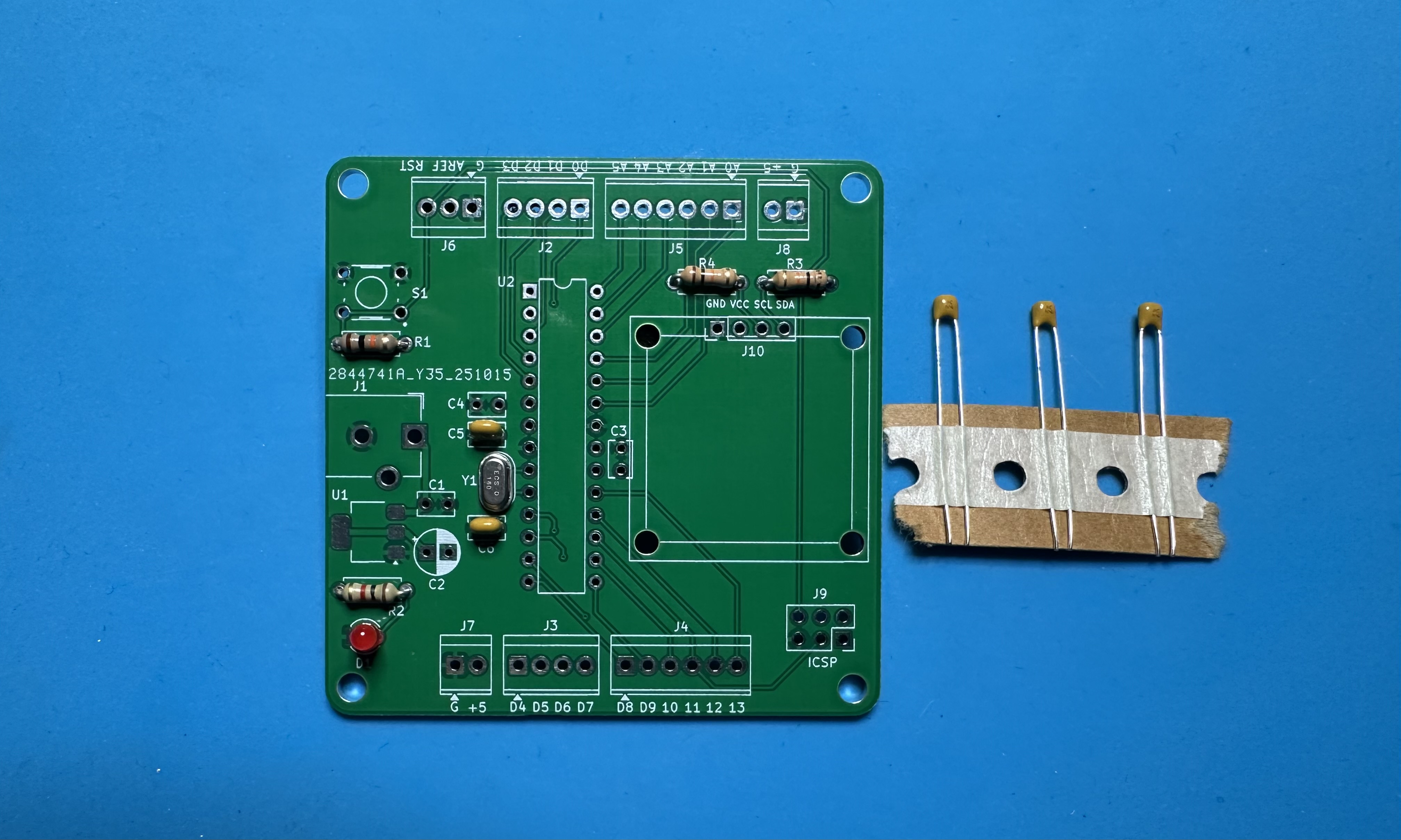
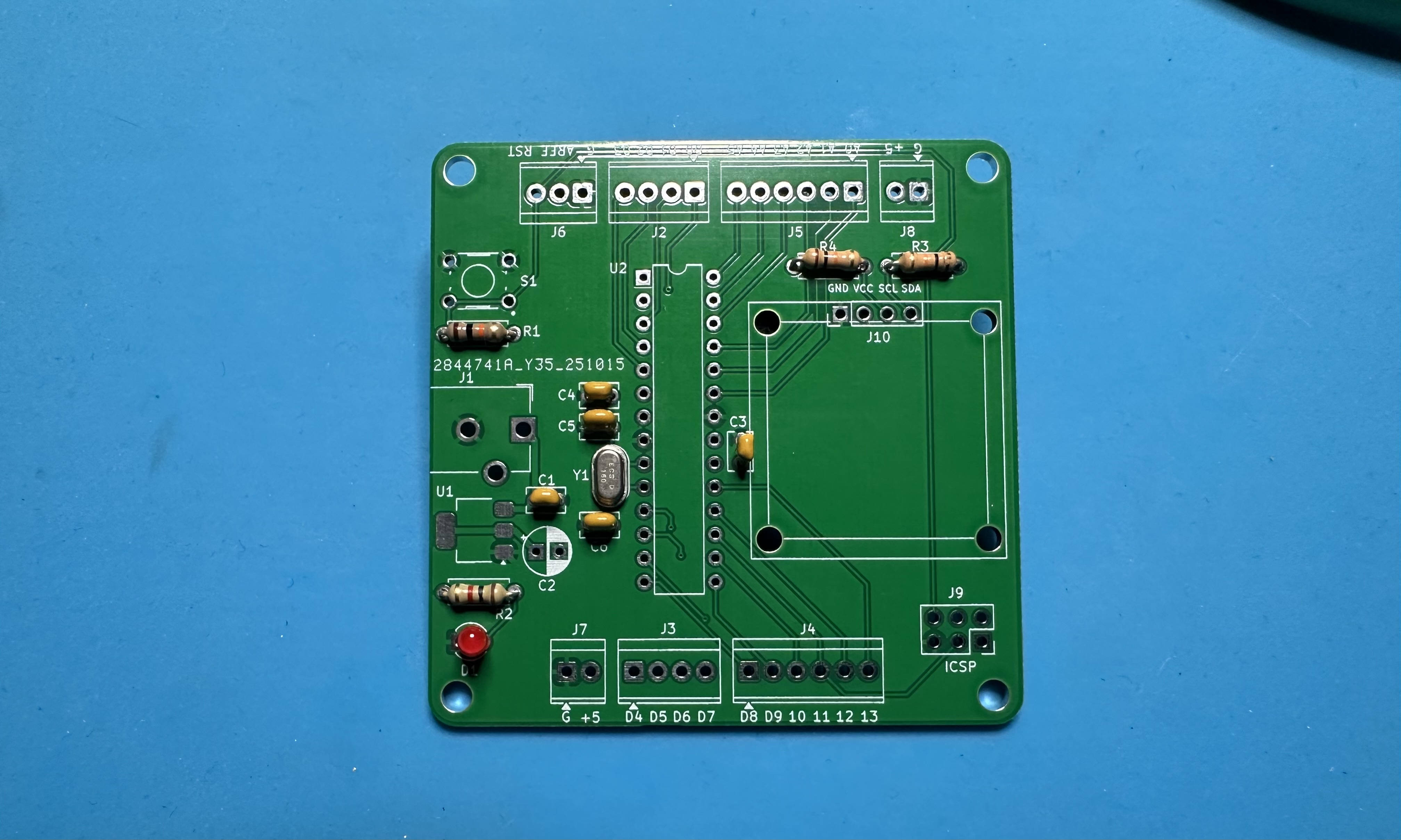
- Start small. Solder in three 10-kΩ resistors (5%, brown-black-orange). Two are pullups for the I2C serial communications channel (R3 and R4), and one is the pullup for the Atmega reset (R2).
- The power-indicator LED, D1, and the 1-kΩ limiting resistor, R1 (brown black red). The LED is directional — it must be soldered in with the correct orientation. The longer lead is the anode (positive) and goes in the circular through hole. The shorter lead is the cathode (negative), and it goes in the hole with the square outline.
- The 16-MHz oscillator crystal (Y1) for the microcontroller and the two 22-pF (22J) tuning capacitors (C5 and C6).
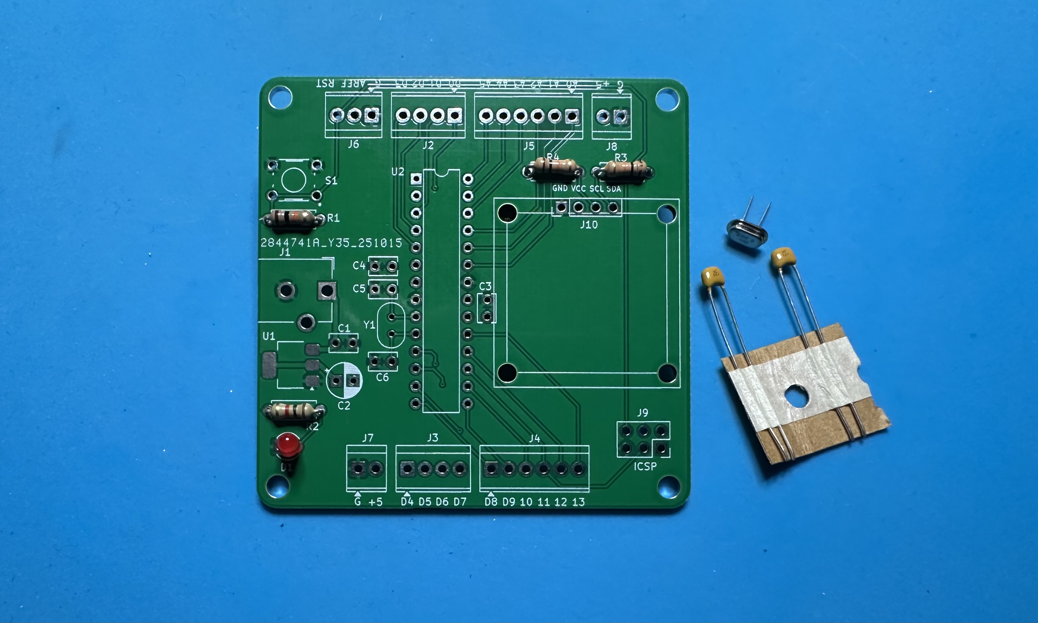
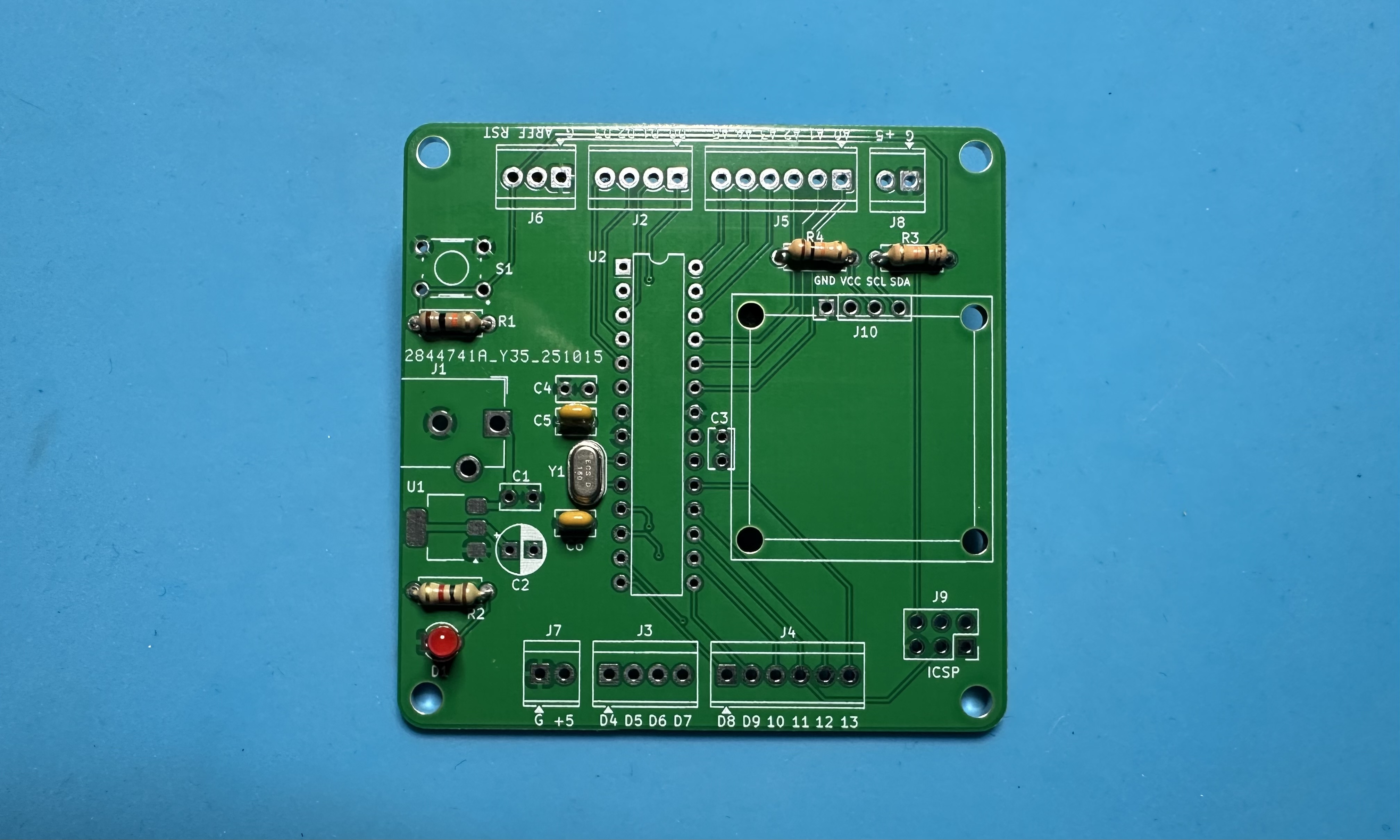
- Three 100-nF (104) capacitors — two for Atmega bypassing (C3 and C4) and one for the input of the voltage regulator (C1).
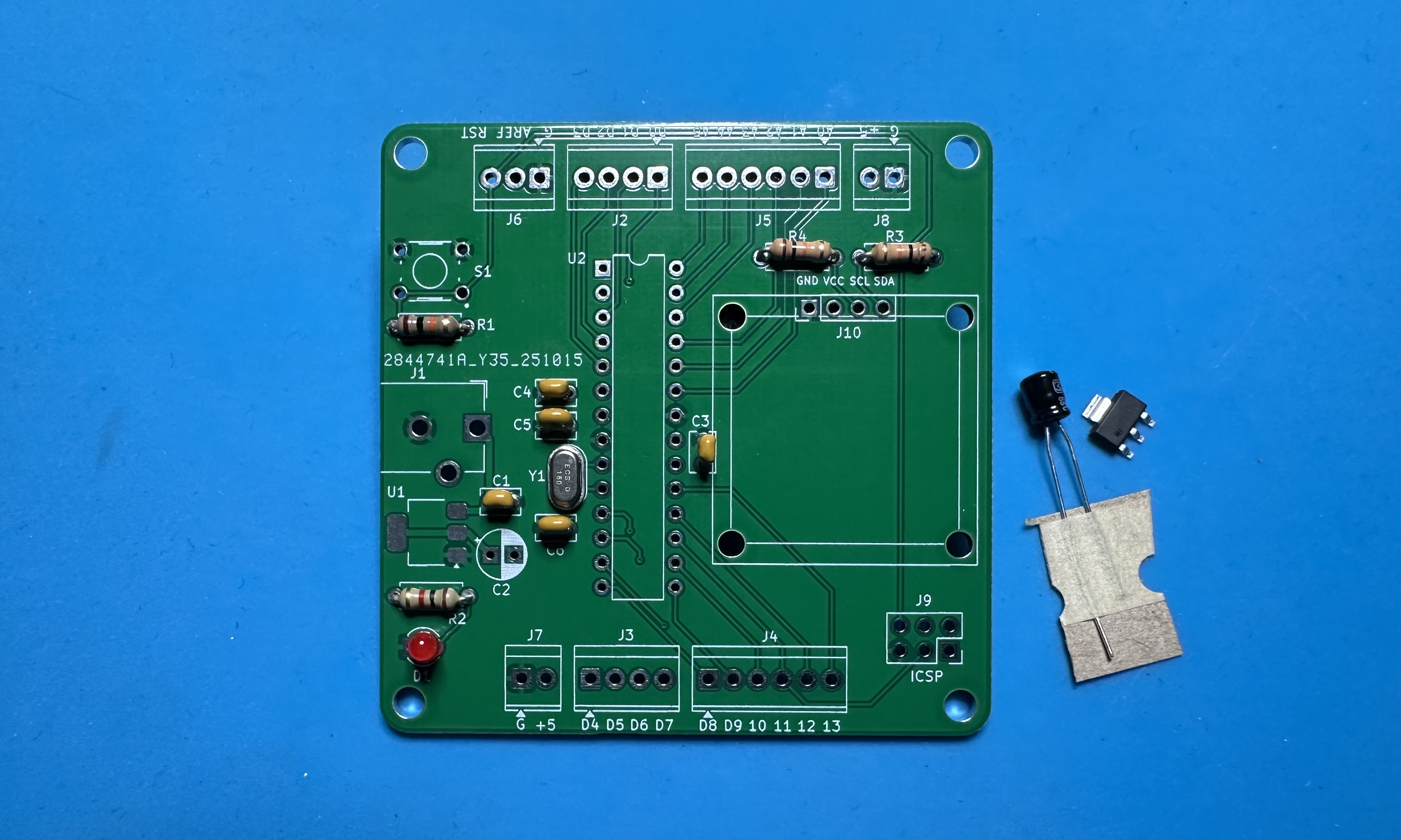
- The LD1117 voltage regulator, U1 and the 10-µF capacitor, C2. The capacitor is electrolytic and must be installed with the correct polarity. We note something new with the voltage regulator — it is a surface-mount part and has no through-hole leads. To solder it:
- Put a small amount of solder one of the pads on the board. It doesn't matter which pad.
- Hold the regulator on the footprint — using needle-nosed pliers or tweezers might help — and remelt the solder on the one pad so that it reflows over the corresponding lead.
- After the solder has cooled, check the alignment of the other leads to the pads. If the alignment is off, the re-melt the solder and adjust the positioning. Repeat as needed until the leads and pads are well aligned.
- Solder the remaining leads.
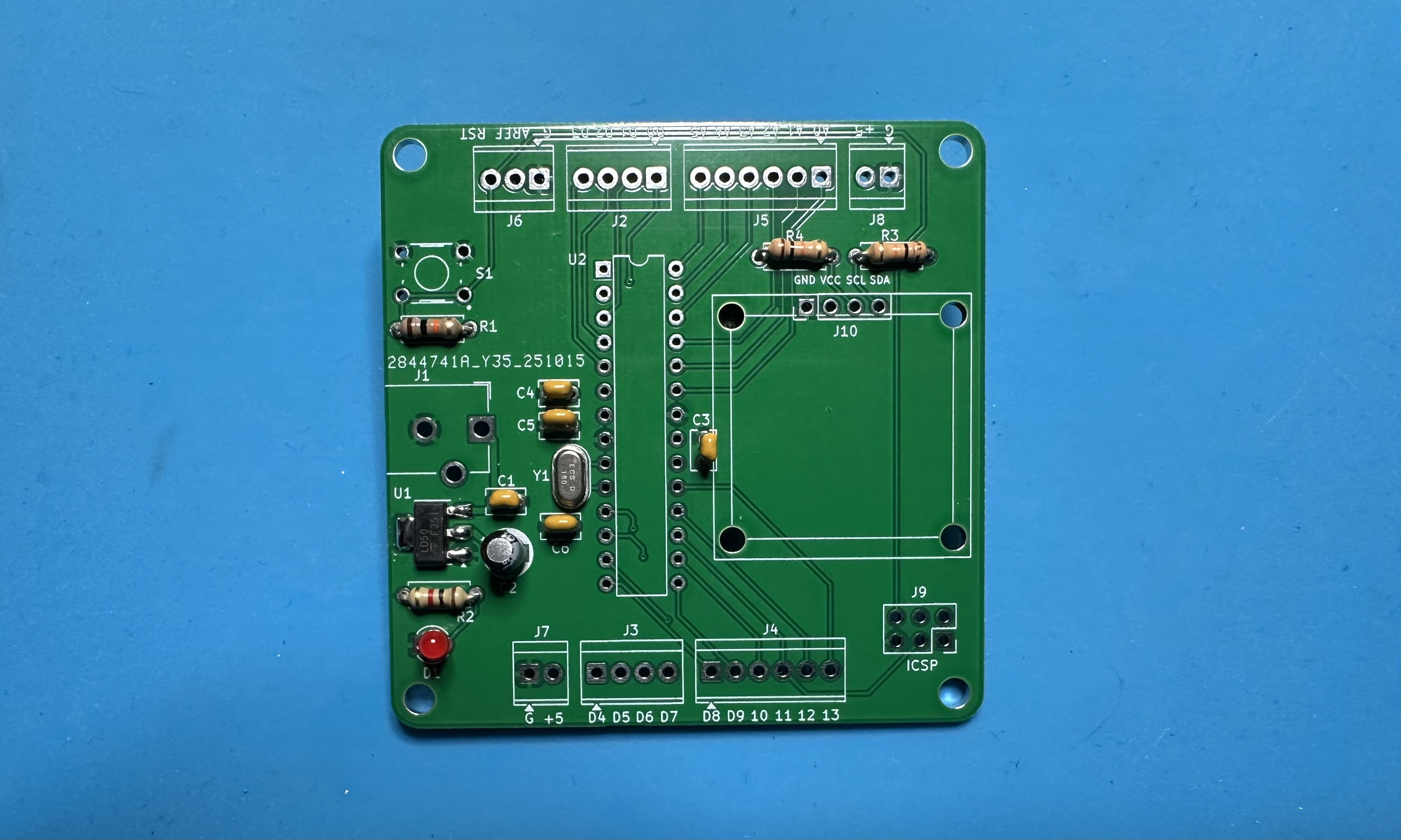
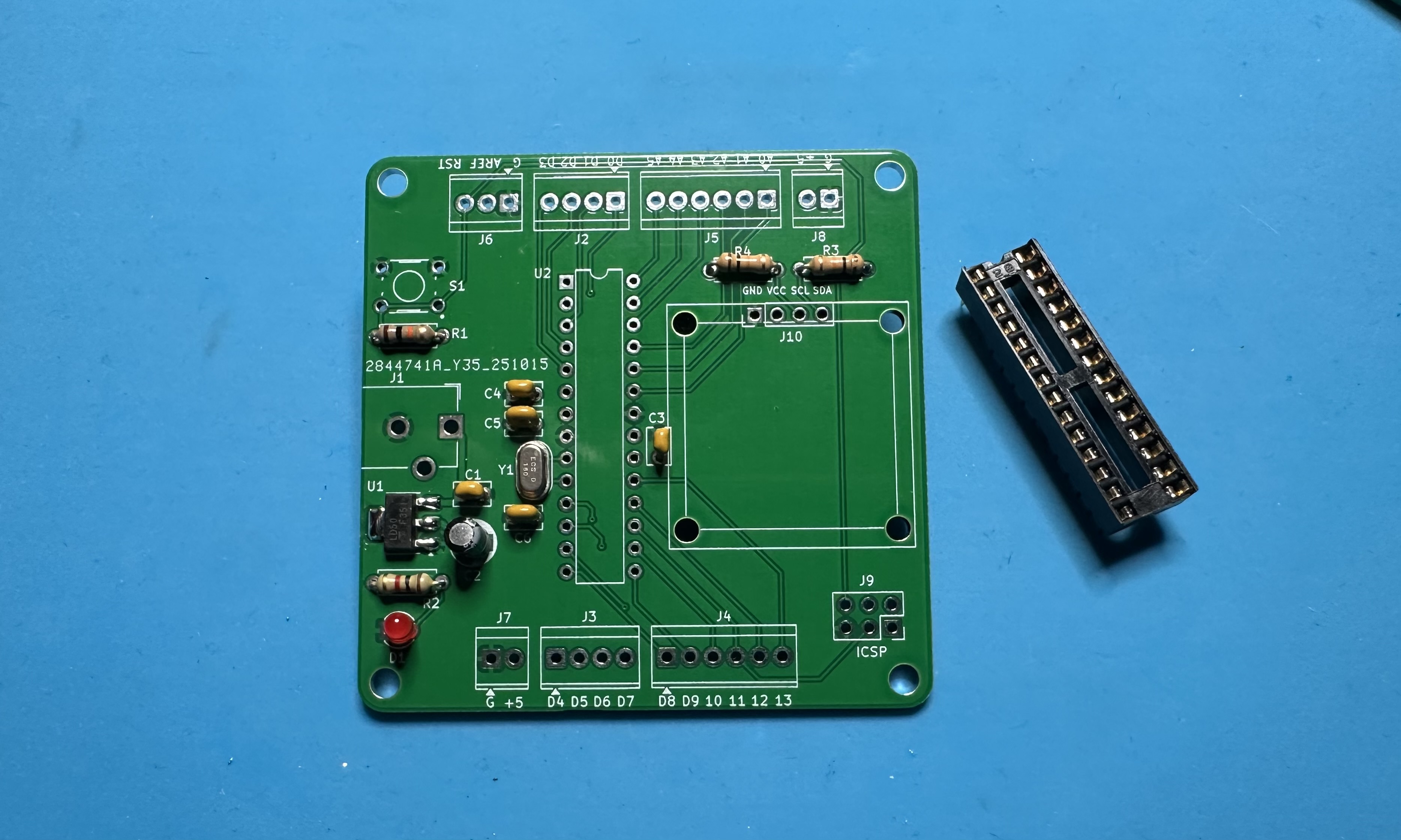
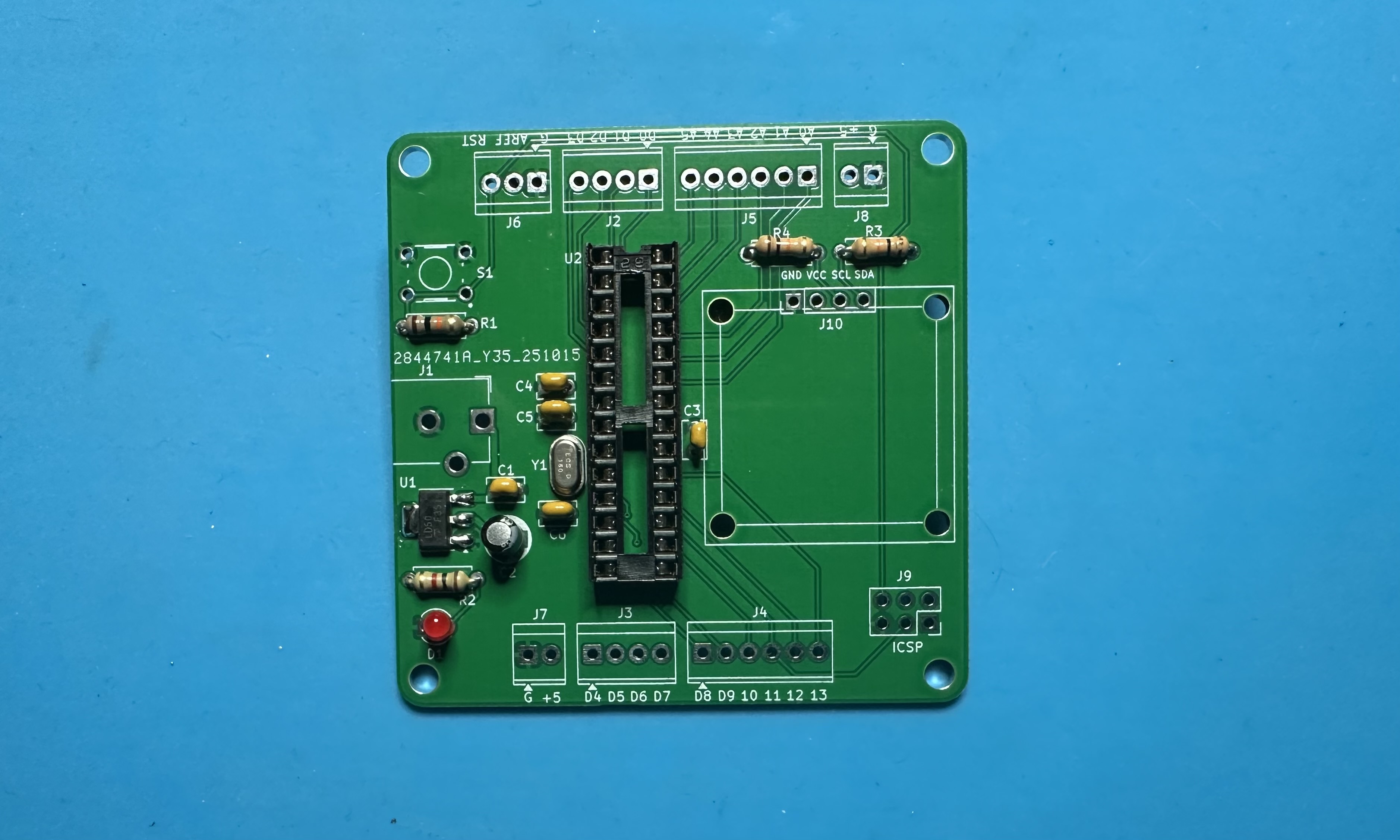
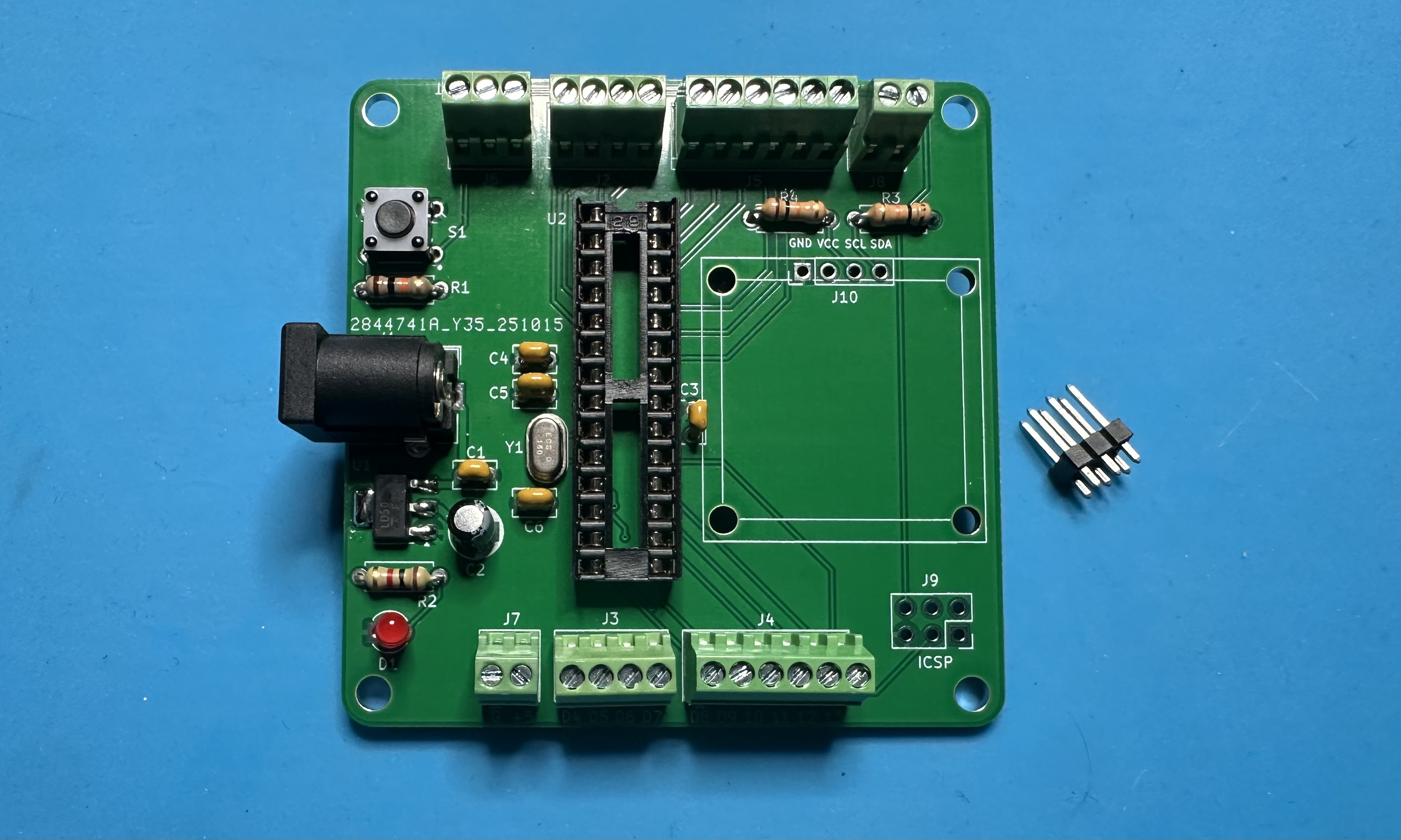
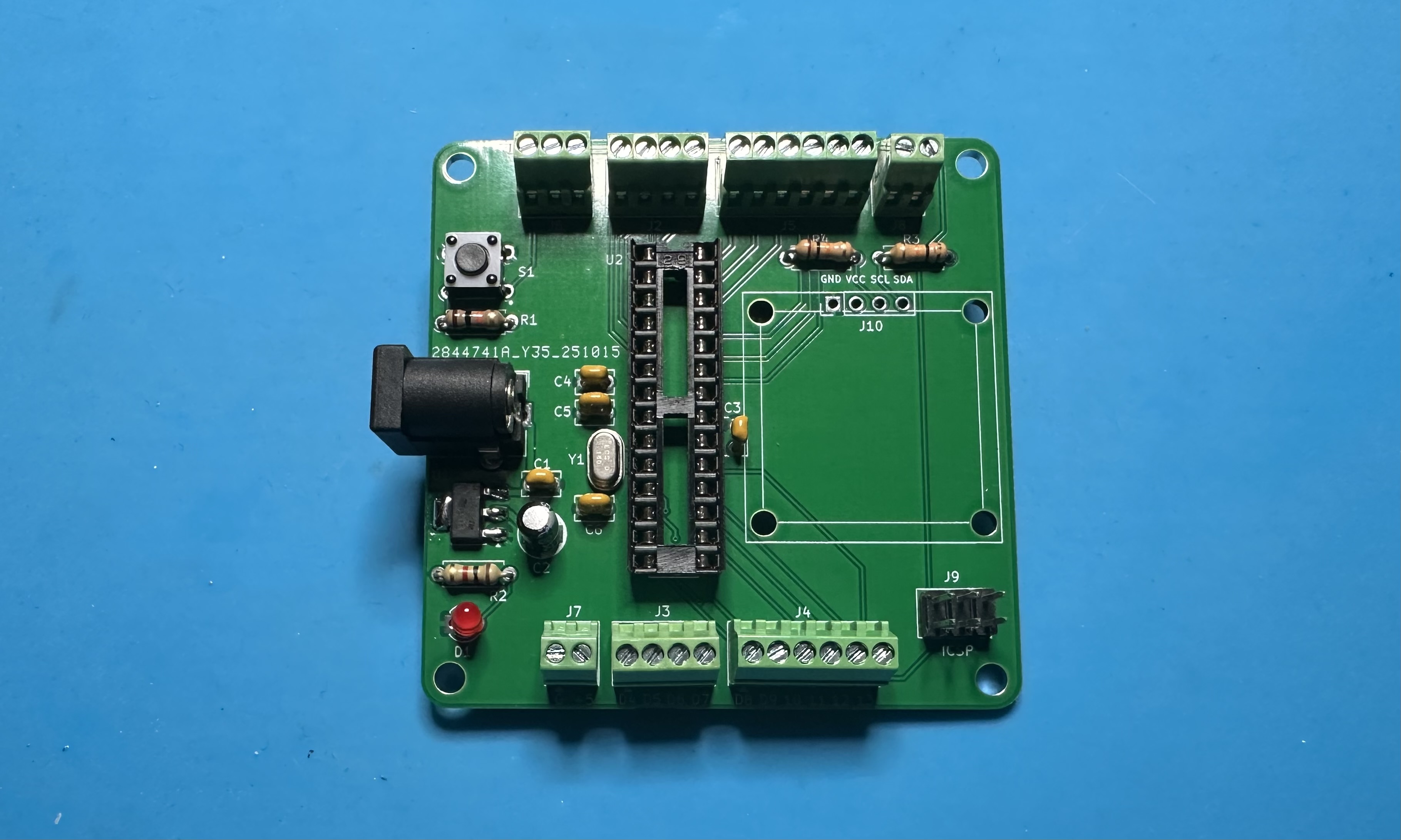
- The chip socket — (U2) for the Atmega chip. This one is tedious — 28 pins. Solder one pin and check the alignment. Then solder the other 27. Take a break!
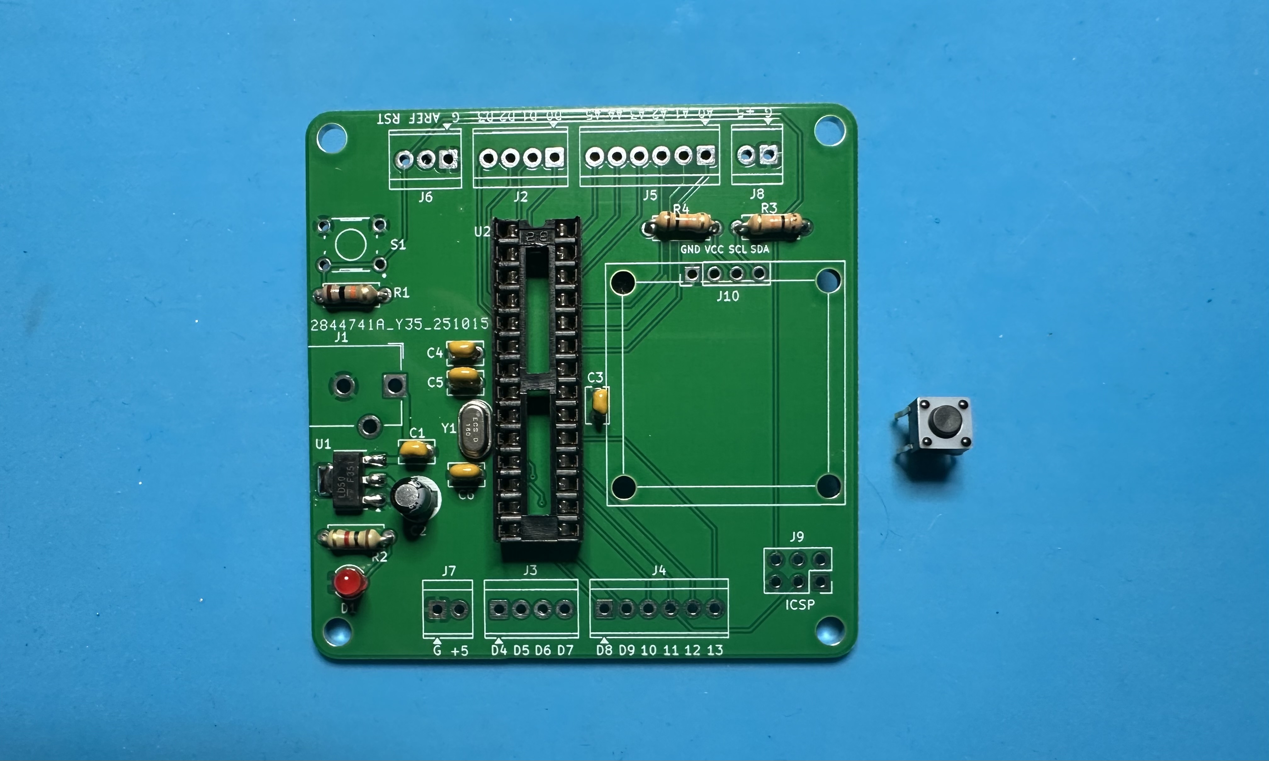
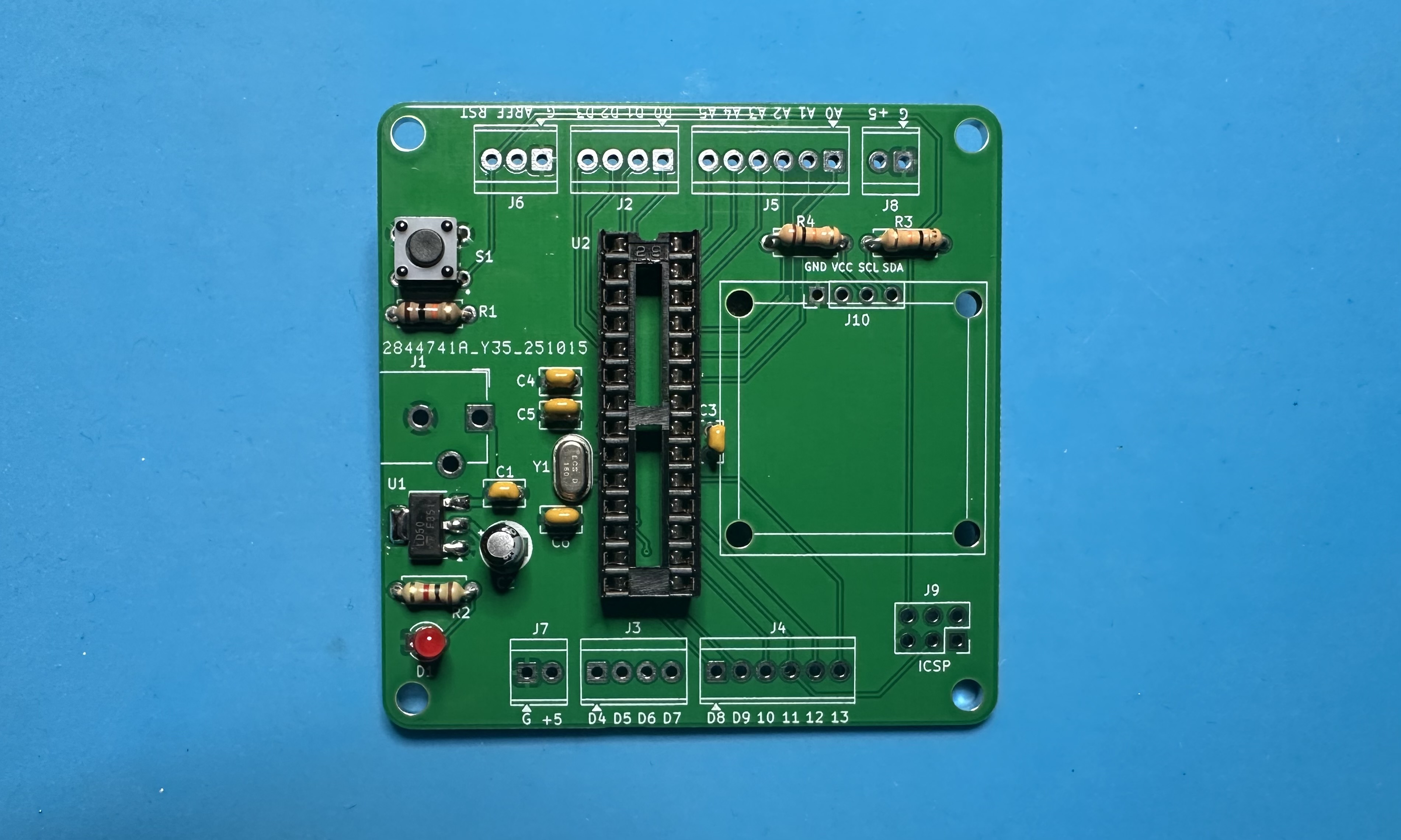
- The momentary switch for chip reset. Fitting the pins can be a bit fiddly. Even though the body of switch is square, the pins are not at the corners of the square — the "up/down" separation is different from the "left/right" separation. Once you get the right orientation, the pins should fit into the through holes. But if needed, use pliers to straighten the pins a bit. The switch symmetric — it can be rotated by 180°, and it will still work.
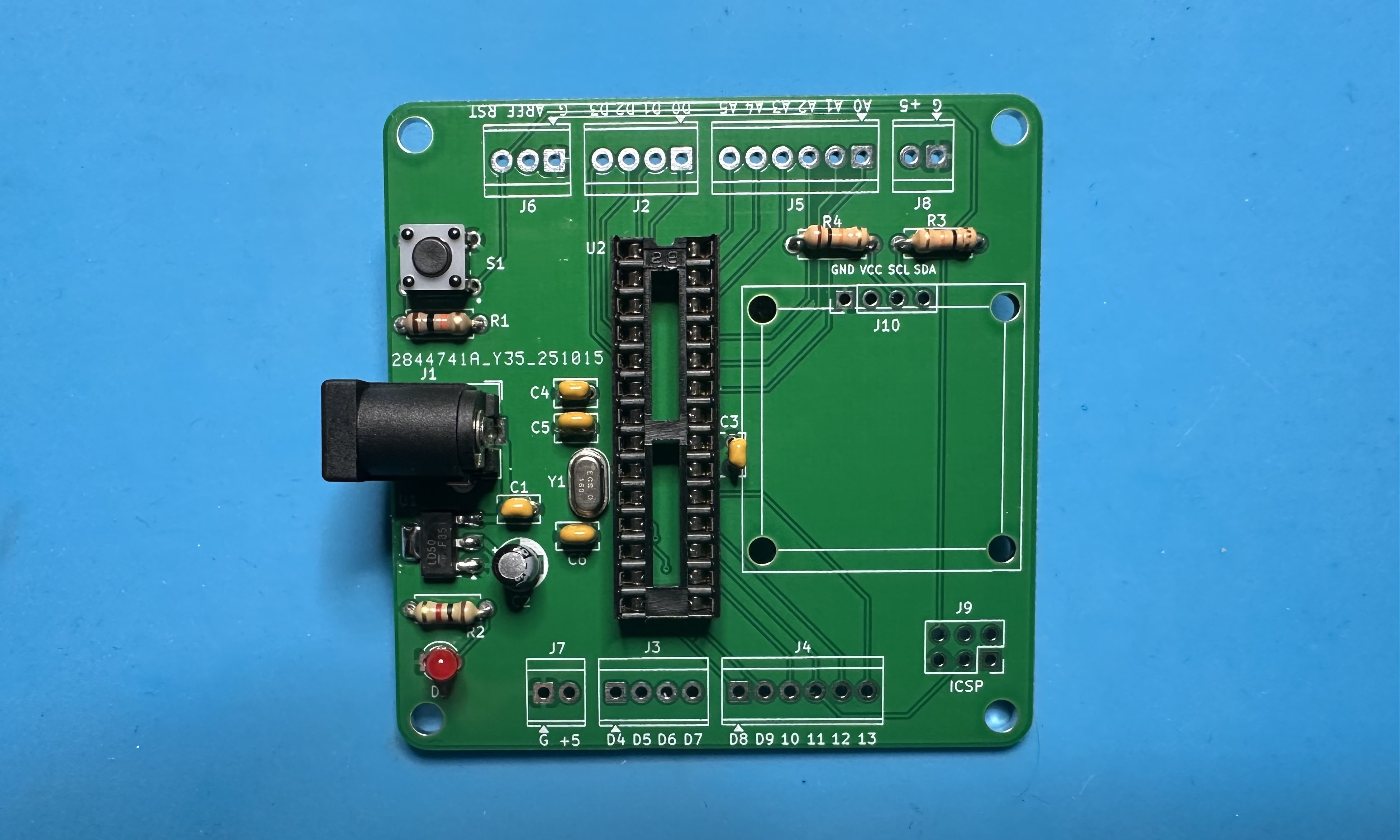
- The barrel jack for power input.
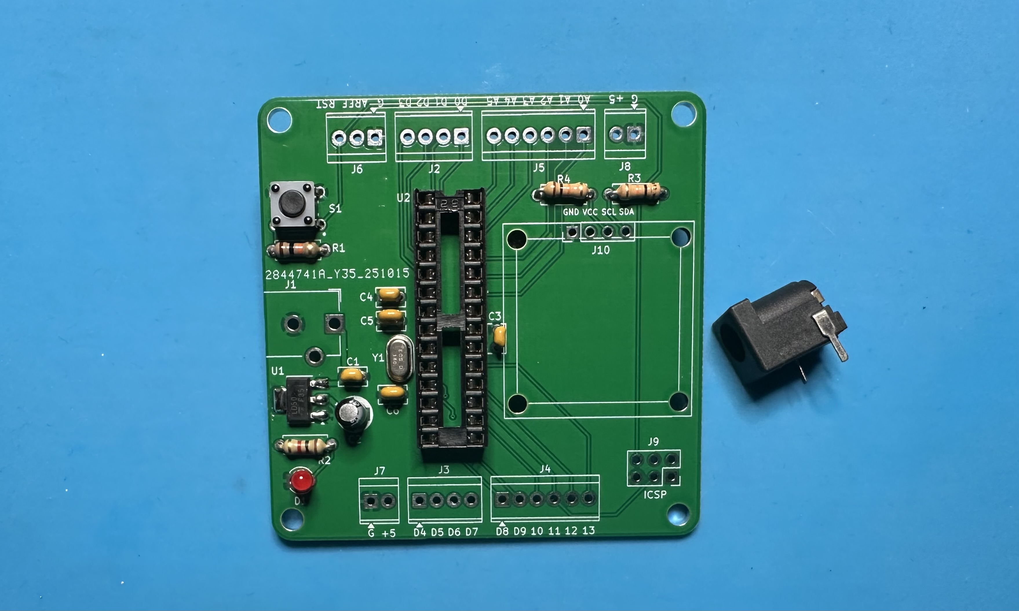
- Seven terminal blocks.
- Two two-position, J7 and J8. Both are for power and ground connections.
- One three-positon, J6. For AREF, RESET, and another ground.
- Two four-position, J2 and J3. For digital connections D0-D3 and D4-D7.
- Two six-position, J4 and J5. For digital pins D8 - D13 and analog pins A0-A5.
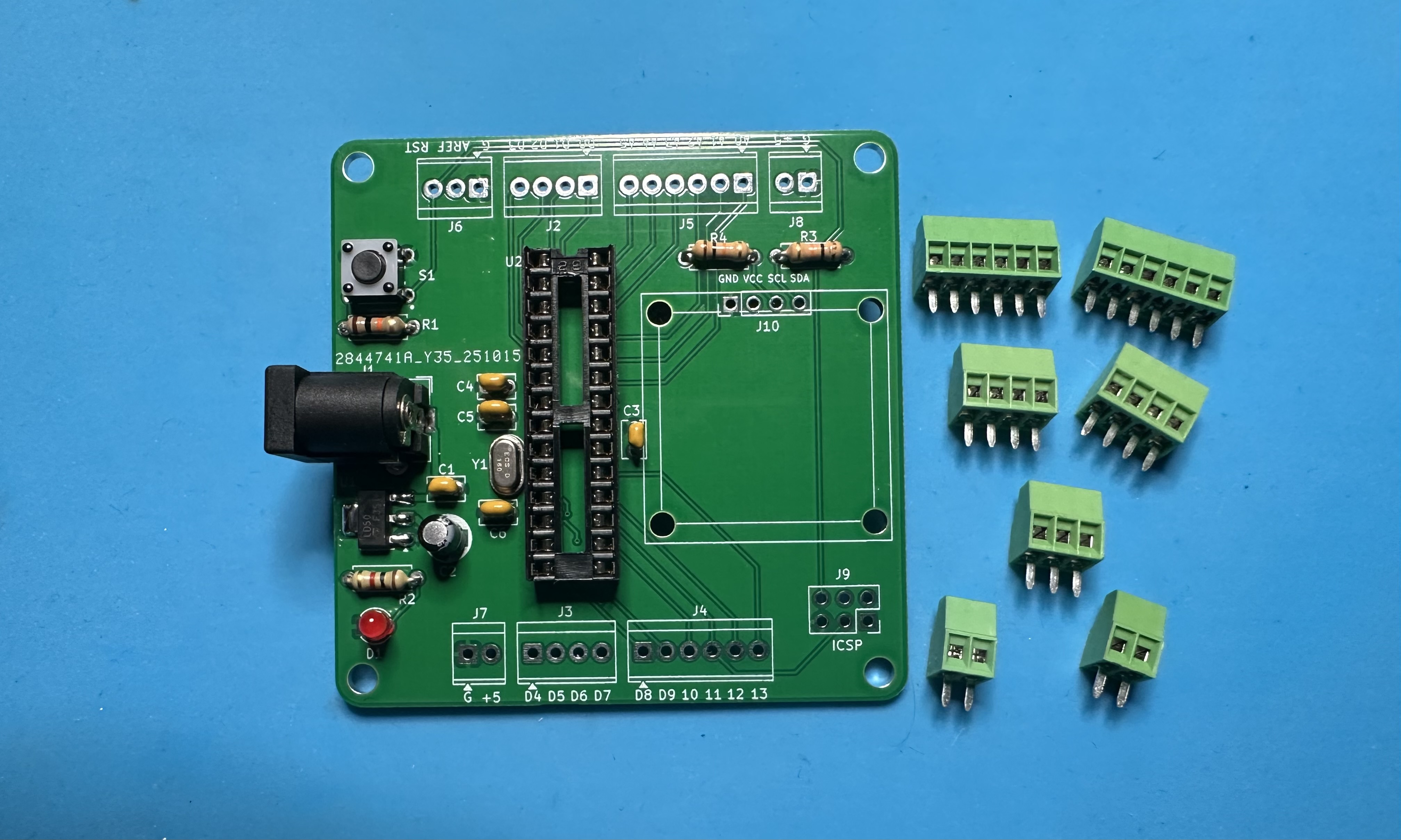
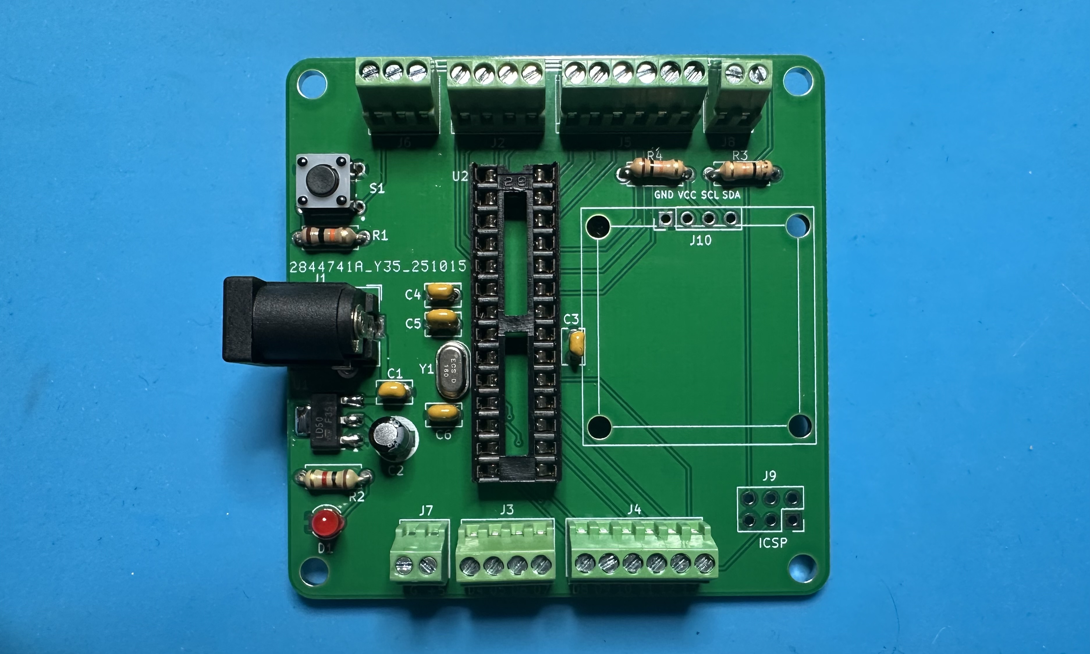
- The six-pin ICSP header, J9, for external programming.
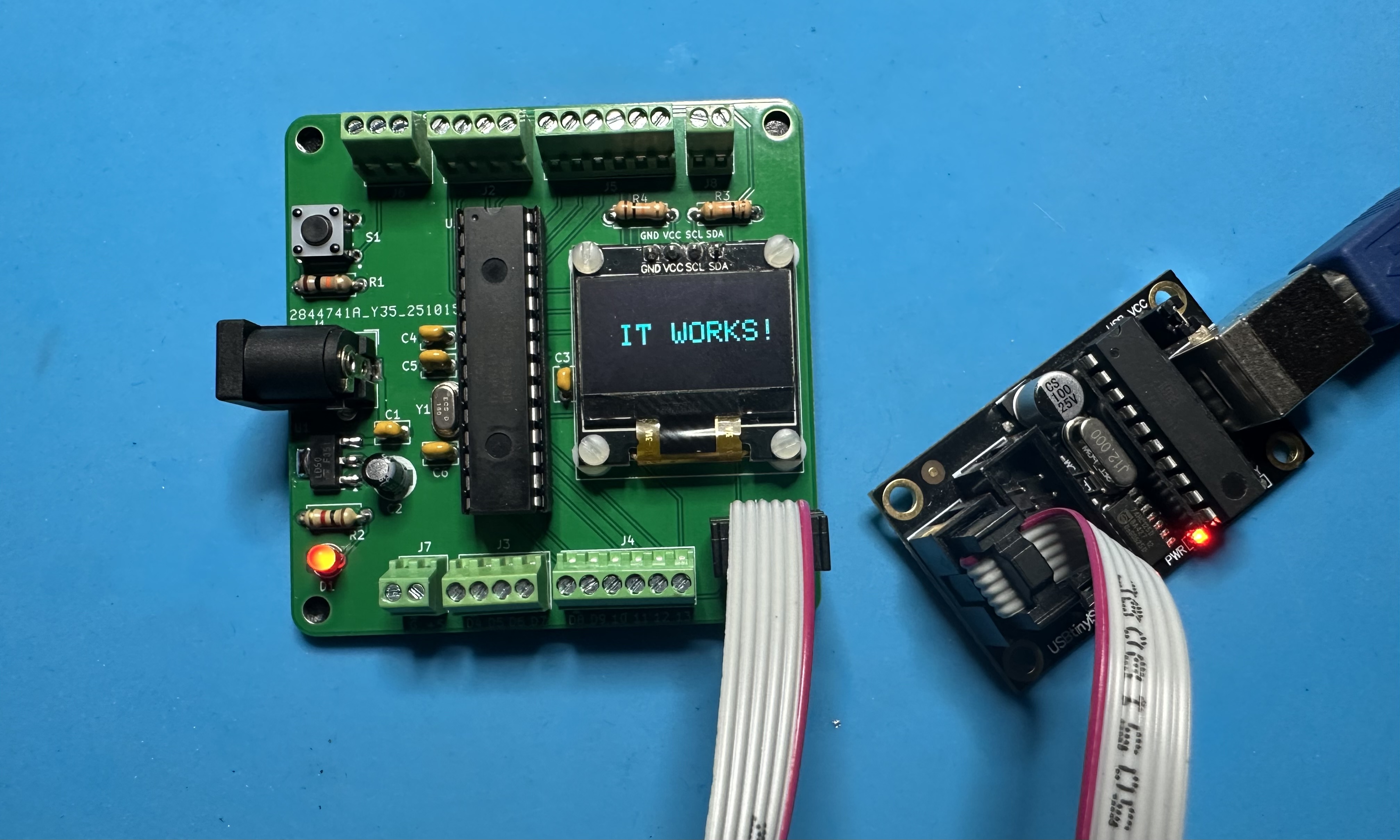
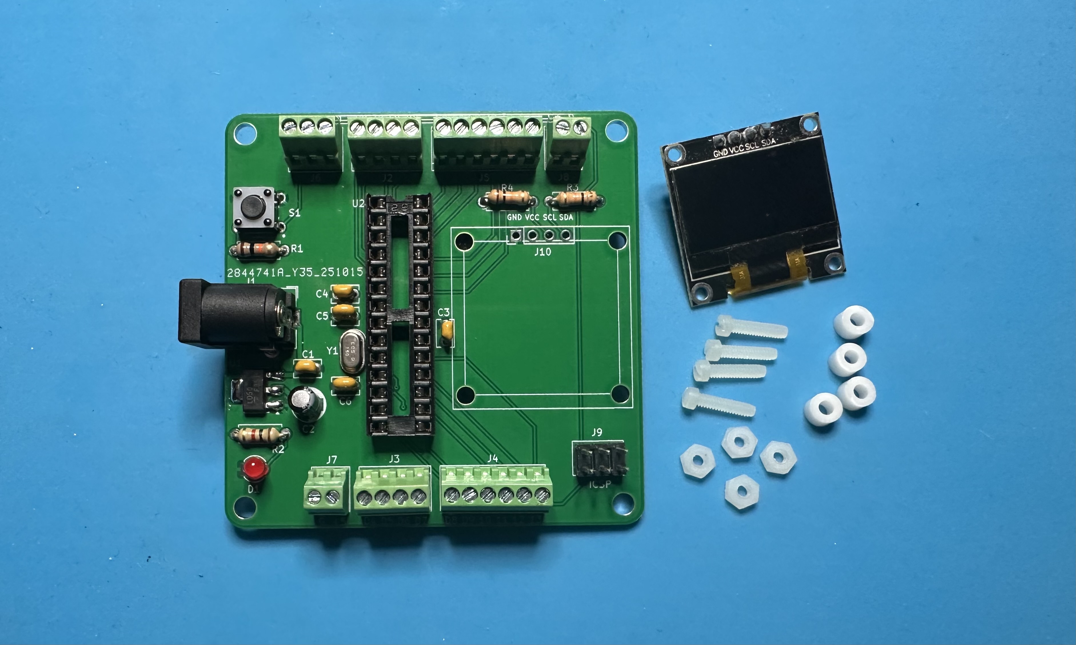
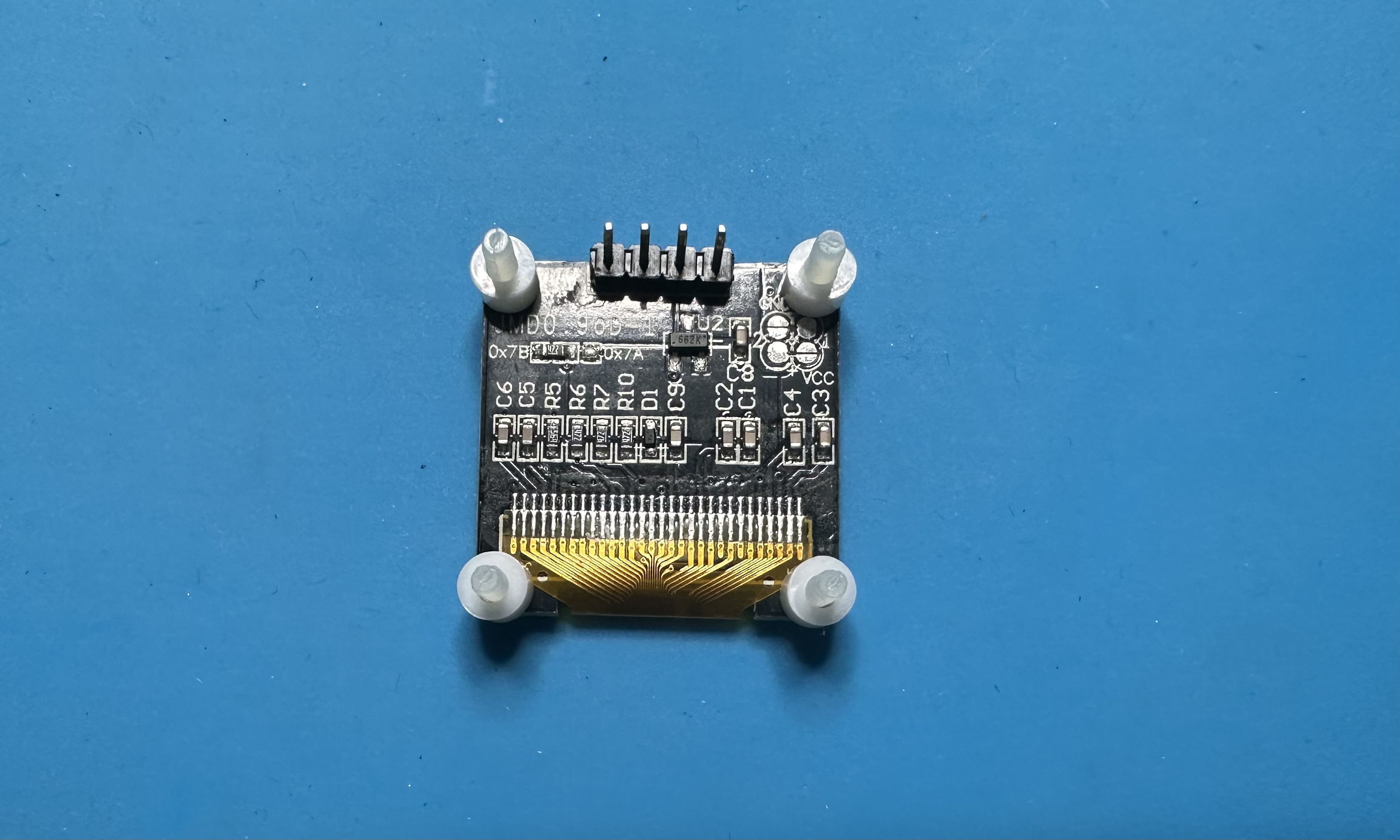
- We are ready to attach the OLED display and solder it in place. Suggested approach:
- Push the four of the nylon screws through the holes of the OLED board. It's a tight fit and you will need to apply a bit of force to get the screws through — the threads should be fine.
- Turn the display over and put the four spacers on the screws.
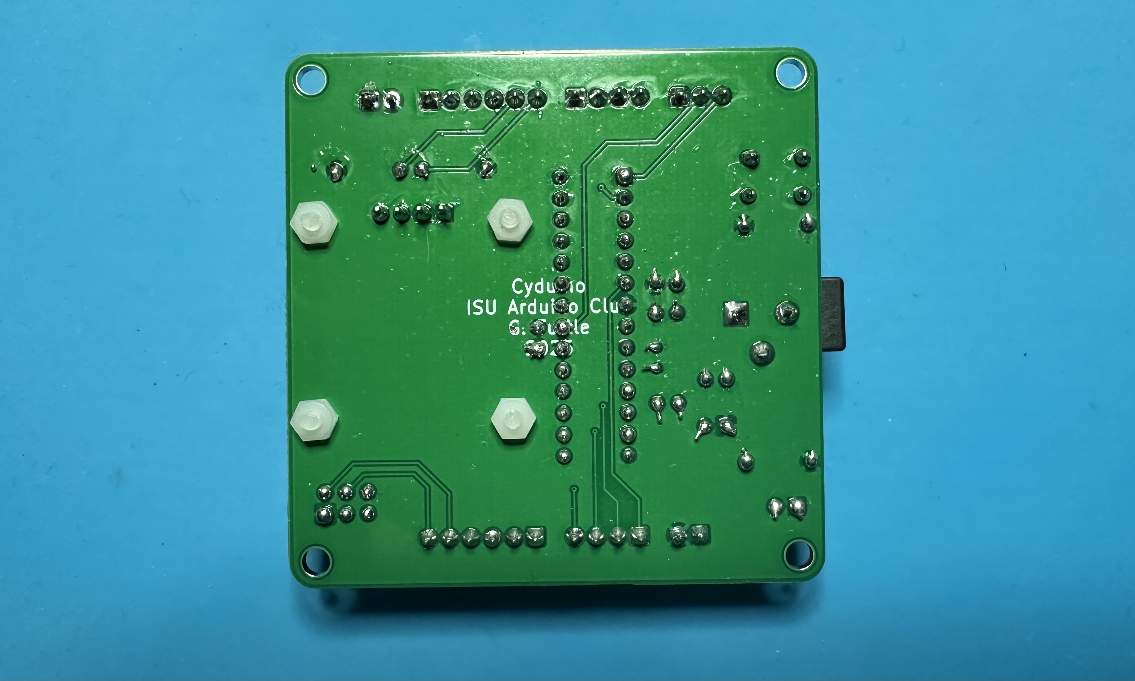
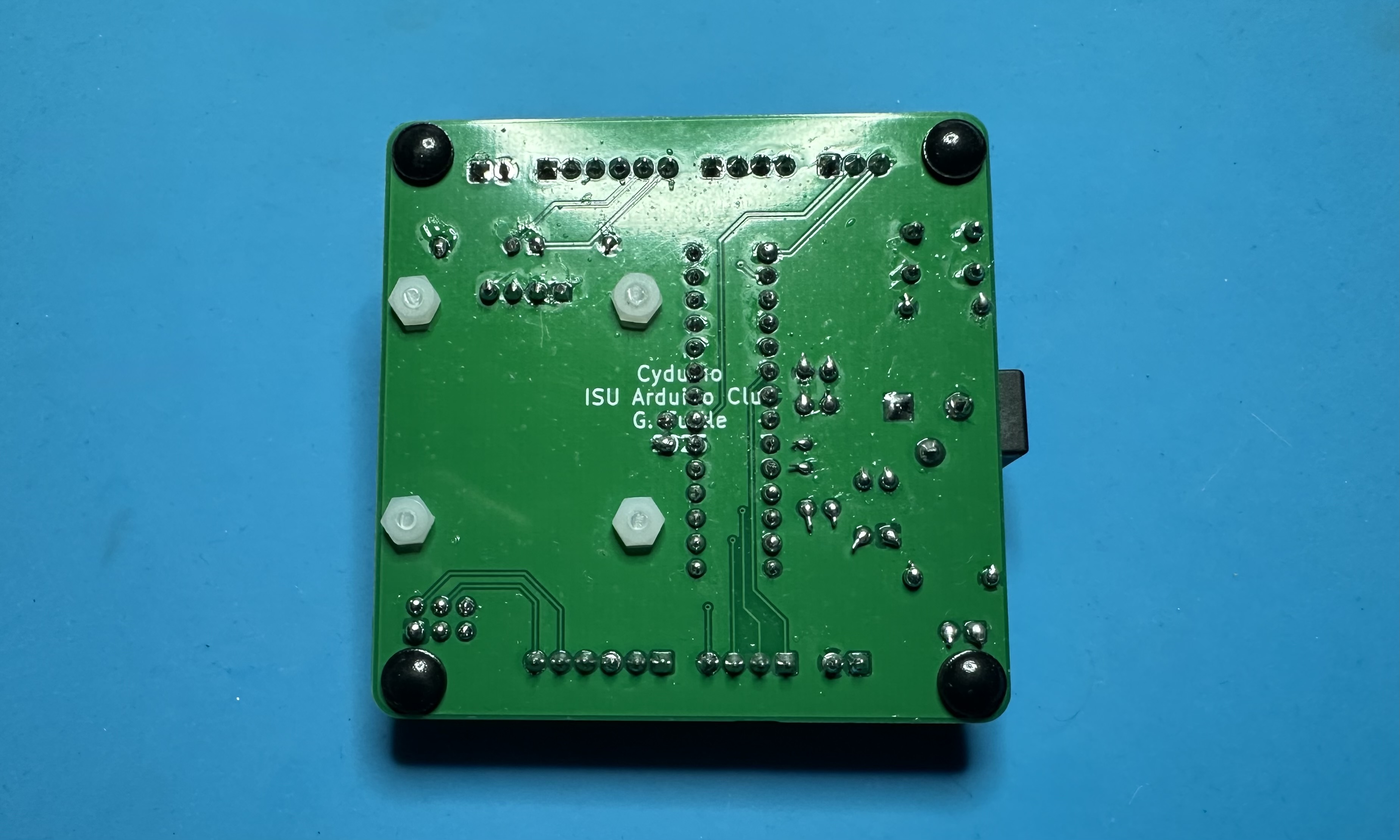
- Turn the PCB over and guide the four holes over the screws. This may require a bit of jiggering in order to align the screws and the OLED pins simultaneously. Secure the OLED to the board by threading four nuts onto the screws — use a screw driver to tighten everything up.
- Finally, solder in the four pins for the display.
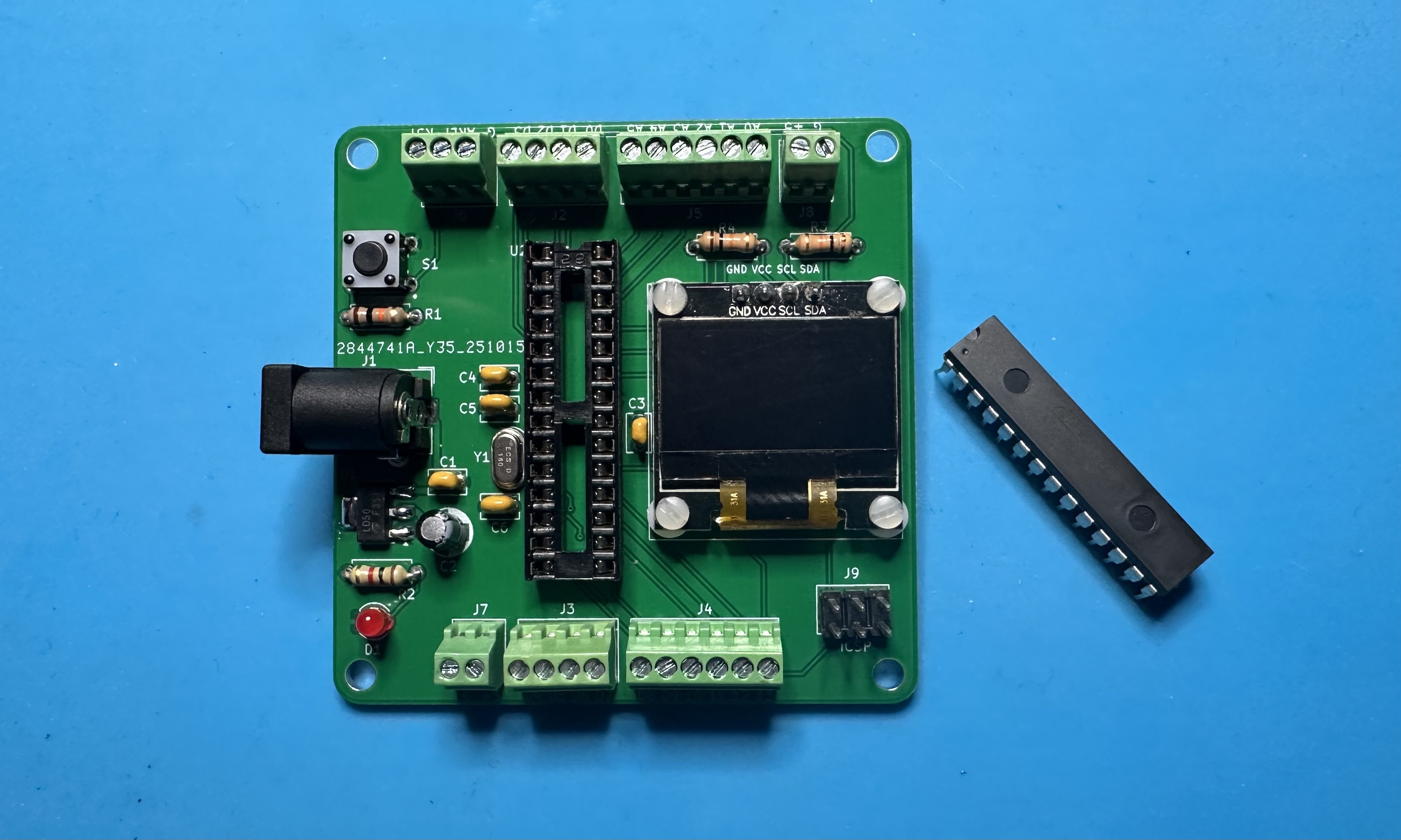
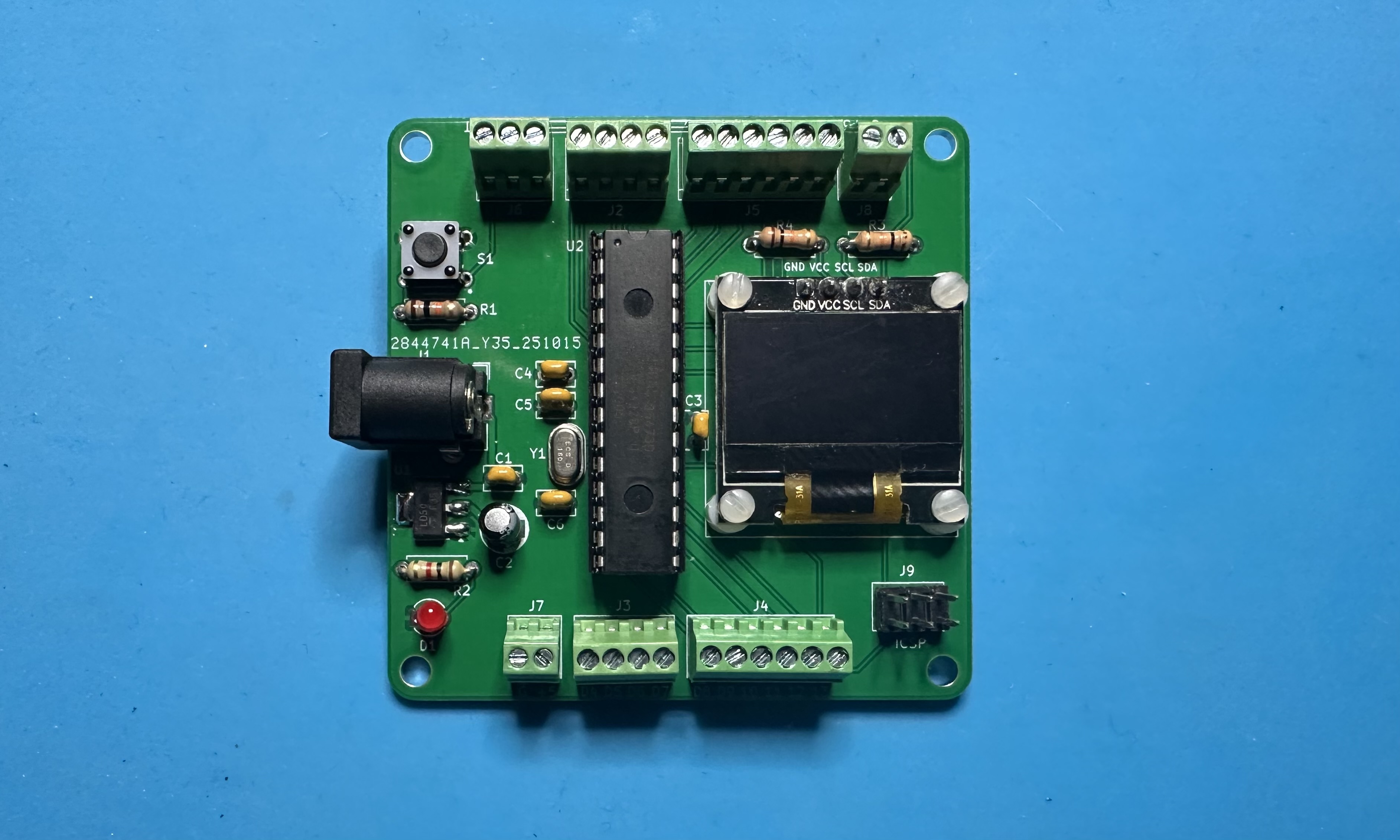
- To finish up, insert the Atmega328 chip into its socket. (Program it first, if you want.) As is typical, you may need to bend the pins inward a bit in order to get the chip to fit into the socket. Proceed carefully.
- If you'd like, attach 4 bumper feet to the bottom corners, so that the board sits level when you are using it. The bumpers won't be effective unless you trim off the excess length of the screws and the OLED leads. Wire cutters work fine for trimming the nylon screws.
- That's it! You are ready to prototype.